

Your PCB fails because invisible pathways inside it got damaged. This loss often destroys expensive projects needlessly. Fixing your board starts by understanding these silent highways.
A PCB trace is a thin copper pathway on a circuit board. It transfers power and signals between components like tiny roads. Every trace must carry current without overheating or breaking to keep devices functional.
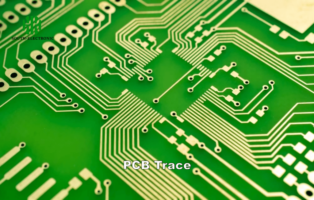
Now that we’ve defined traces, let’s explore why they fail and how to fix them. Proper trace design prevents costly mistakes.
Why is Impedance Critical?
Signal chaos makes your circuit act unpredictably. Mismatched impedance causes data errors and device crashes. Correct it before your project fails.
Control impedance to prevent signal reflections and distortion. Unbalanced paths create ghost signals disrupting communication. I match impedance using trace width calculators to maintain signal quality.
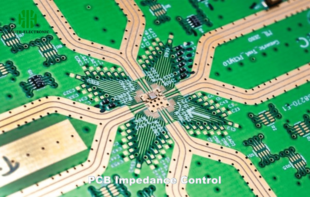
Impedance Factors and Solutions
Three key factors influence trace impedance: trace width, material properties, and path distance. Let’s break them down.
First, trace dimensions are critical. Wider paths lower impedance – narrower paths raise it. Use a pcb trace width calculator to balance size requirements. Here’s a typical impedance relationship:
| Trace Width (mm) | Impedance (Ohms) |
|---|---|
| 0.2 | 70 |
| 0.3 | 55 |
| 0.5 | 45 |
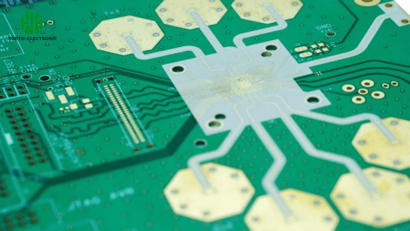
Second, board material matters. FR4 substrates have higher dielectric constants than specialty materials. Thinner dielectrics increase impedance values.
Ground plane distance forms the third factor. Traces closer to ground planes exhibit lower impedance. My rule: place power traces nearer to reference planes than signal traces. This planning avoids cross-talk disasters.
Always verify with a trace width calculator for pcb before manufacturing. An impedance mismatch caused my prototype to repeatedly crash until I rerouted signals using copper width adjustments.
Is My PCB Trace Too Hot?
Hot traces cause mysterious circuit shutdowns. Overheating copper melts solder joints. Detect thermal issues before components burn.
Measure trace temperature during operation. Excess heat means incorrect sizing. I prevent meltdowns using a pcb trace current calculator during design.

Causes and Preventive Measures
Trace overheating stems from current overload and poor design. Here’s how to protect your board.
Resistance generates heat. Thin or long pcb trails create higher resistance. Doubling trace width doubles current capacity. Use this table to avoid thermal failures:
| Current (A) | 1oz Copper Width (mm) | Temp Rise (°C) |
|---|---|---|
| 1 | 0.3 | 10 |
| 3 | 1.0 | 15 |
| 5 | 2.0 | 20 |
External factors worsen overheating. Poor airflow traps heat near components. My prototype once failed because I ignored environmental controls. Now I simulate heat patterns using pcb trace calculators.
Preventive steps save boards: increase copper weight for high-power traces, avoid right-angle corners, and use pcb trace width current calculators during layout. Thermal relief patterns help dissipate heat effectively.
PCB Trace Troubleshooting Guide
Frustrated with dead boards? Broken traces stop signals cold. Find faults quickly before wasting repair time.
Check traces systematically with visual inspections and tools. My four-step method revives damaged boards every time. Always have a pcb trace repair kit ready.
Diagnostic Tools and Repair Steps
Trace failures demand proper troubleshooting. Gather essential tools to fix pcb trace errors.
Critical tools:
- Microscope
- Multimeter
- Conductive pen
- pcb circuit trace repair kits
Follow this workflow:
| Step | Action | Tool Required |
|---|---|---|
| 1 | Visual inspection | Microscope |
| 2 | Continuity check | Multimeter |
| 3 | Expose copper | Fiberglass scrubber |
| 4 | Bridge gap | Repair kit/silver epoxy |
First, locate physical damage under magnification. I once found micro-cracks invisible without a microscope. Next, test conductivity across traces using a multimeter. Missing continuity confirms breaks.
Scrape solder mask to expose copper on both break sides. Then apply conductive epoxy from a quality pcb trace repair kit. I always test repairs under load to prevent future failures.
For severed power traces, double-check calculations using a trace current calculator afterward. This ensures the repaired trace can handle the required current and won’t overheat again.
Conclusion
Master pcb trace design and repair for reliable electronics. Understanding trace properties prevents overheating and signal loss. Your circuits will operate flawlessly every time.


