
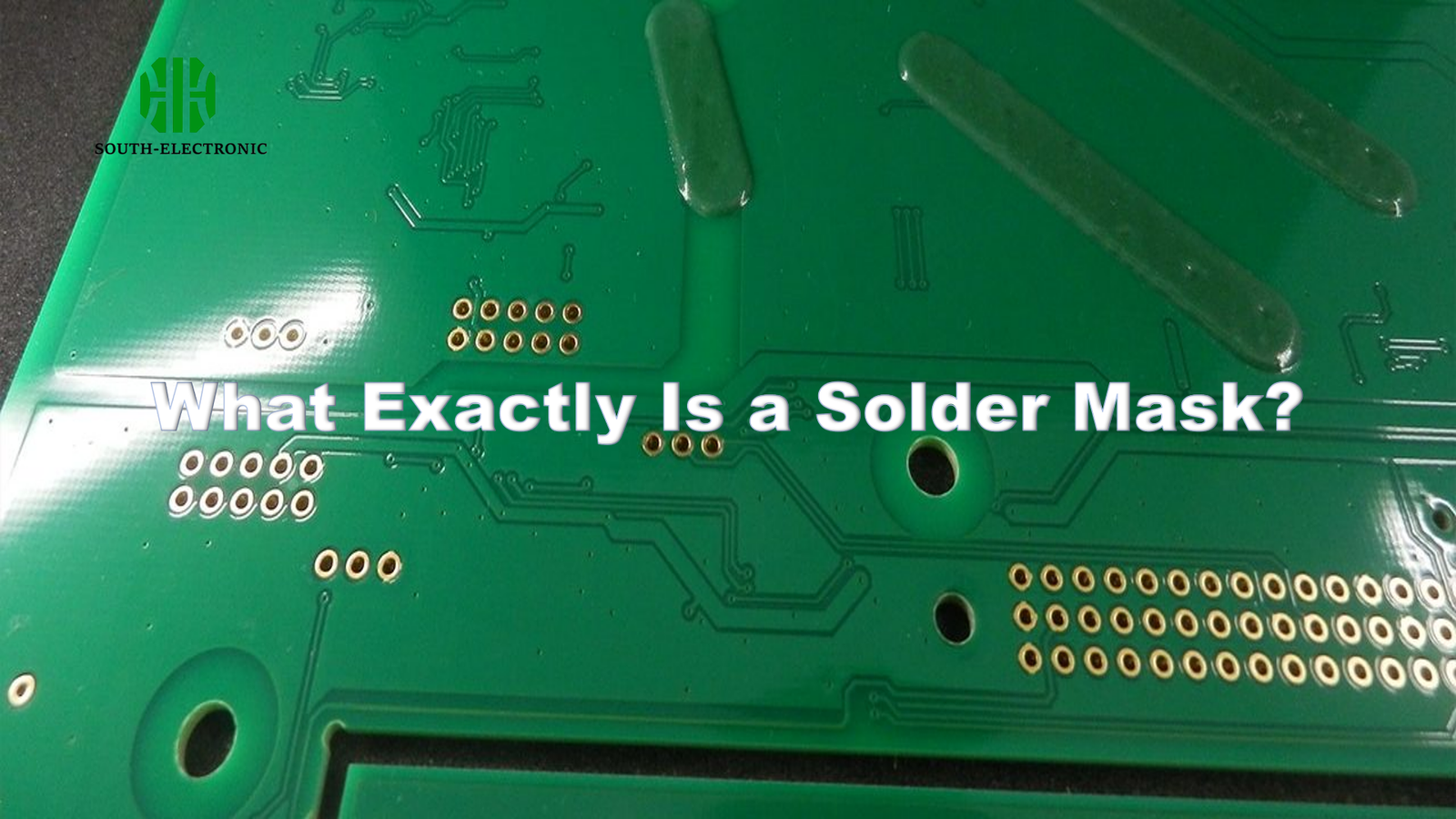
Ever noticed blobs of solder causing chaos on your circuit board? Short circuits and damaged components frustrate every engineer. A solder mask solves this nightmare.
A solder mask is a polymer layer applied to PCB surfaces that blocks uncontrolled solder flow. It exposes only designated pads/vias through openings, preventing solder bridges and environmental damage to copper traces.

Now, let’s explore why this thin layer matters more than you think, and how it transforms basic PCBs into reliable devices.
Why is Solder Mask SO Important for Reliable PCB Function?
Imagine soldering tiny components without precision. Solder bridges would cripple half your boards! Protection can’t be an afterthought.
Solder mask prevents electrical shorts, reduces corrosion, provides insulation, and resists chemical/mechanical stress. Without it, 90% of modern electronics would fail prematurely.
Three Pillars of PCB Protection
| Function | Impact | Failure Example |
|---|---|---|
| Electrical Isolation | Blocks accidental connections | Short circuits between adjacent traces |
| Environmental Shield | Prevents oxidation & contamination | Corroded copper traces causing signal loss |
| Solder Control | Confines solder to pads | Solder balls creating false connections |
Solder mask material creates microscopic barriers between conductive elements. The epoxy resin forms a dielectric shield against moisture, dust, and corrosive elements. Thermal stability matters too—quality masks withstand reflow temperatures without cracking. One prototype board of mine shorted because a low-grade material melted during assembly. Beyond electrical safety, the solder mask color (typically green) improves component visibility during manual inspection. Reliability drops 30% in boards lacking this layer—it’s not decoration!
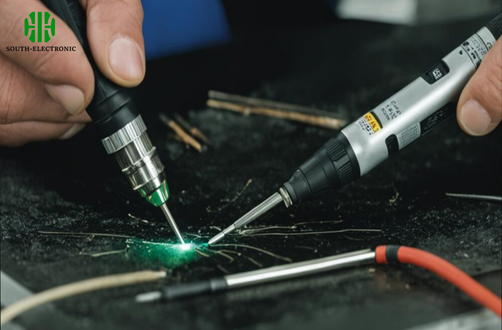
How is Solder Mask Applied?
Ever hand-painted a circuit board solder mask? Industrial application needs surgical precision to avoid costly defects.
Solder mask application involves coating-cleaning, epoxy deposition, UV exposure, development, and curing. Liquid Photoimageable (LPI) epoxy is sprayed or silk-screened, hardened by UV light, with unexposed areas chemically washed away.
Critical Application Stages
| Step | Purpose | Common Pitfalls |
|---|---|---|
| Surface Prep | Clean copper surfaces | Residual oxides cause poor adhesion |
| Coating | Apply liquid solder resist | Uneven thickness creates weak spots |
| UV Exposure | Harden masked areas | Under-exposure leaves residues |
| Development | Remove unhardened resin | Over-etching damages openings |
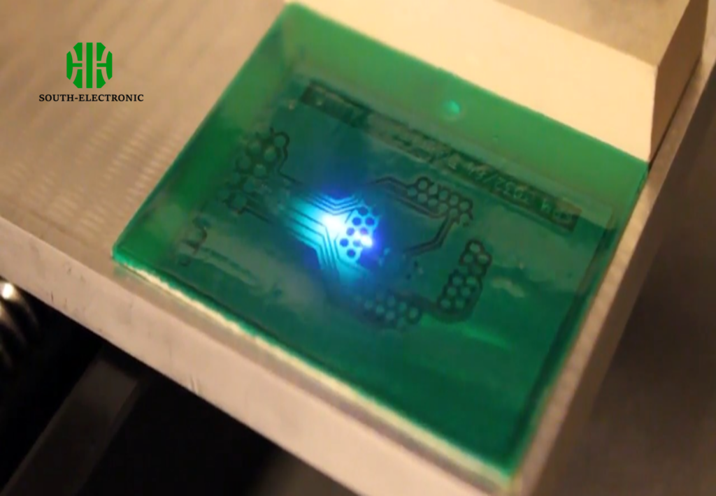
The coating stage determines everything. Spraying suits complex boards, while screen printing is faster for simple layouts. For UV solder mask processing, a phototool blocks light over openings, hardening the insulation areas while keeping pads exposure-ready. When developing, incorrect chemical concentrations can eat into protected zones. One batch we tested had pad gaps 0.1mm undersized due to over-development. Curing provides final hardness—incomplete curing leaves tacky surfaces attracting dust. Newer methods like electrostatic coating reduce material waste.
What Types of Solder Mask Exist & Which is Best for Your Project?
Choosing a soldering mask feels like picking armor—wrong material equals battlefield failure. Trade-offs lurk everywhere.
Primary solder mask materials are epoxy-based Liquid Photoimageable (LPI), solvent-based inks, and dry films. LPI dominates production for cost/resolution balance, while UV-curable masks speed prototyping.

Decision Matrix
| Type | Resolution | Cost | Best Use Case |
|---|---|---|---|
| Epoxy-based LPI | Excellent | $$ | Complex consumer electronics, fine-pitch components |
| UV-Curable | Good | $$$ | Rapid prototypes needing 2-hour turnaround |
| Dry Film | Very High | $$$$ | HDI boards with <50μm openings |
| Acrylic/Polyimide | Moderate | $ | Limited thermal flex PCBs |
Epoxy-based LPI delivers superb chemical resistance and adhesion—it's why 80% of your devices use it. UV solder mask options harden in minutes but often lack LPI’s mechanical strength. For my drone PCBs, UV worked until vibration testing caused peeling. Dry films suit ultra-fine features but demand perfect surface flatness. Aerospace projects benefit from polyimide’s extreme temperature tolerance despite higher costs. Match your selection to these factors: production volume, feature density, thermal needs, and budget.
Conclusion
Solder mask remains the unsung PCB hero. Its functions—short prevention, solder control, and environmental protection—enable reliable modern electronics. Choose wisely for every project.

