

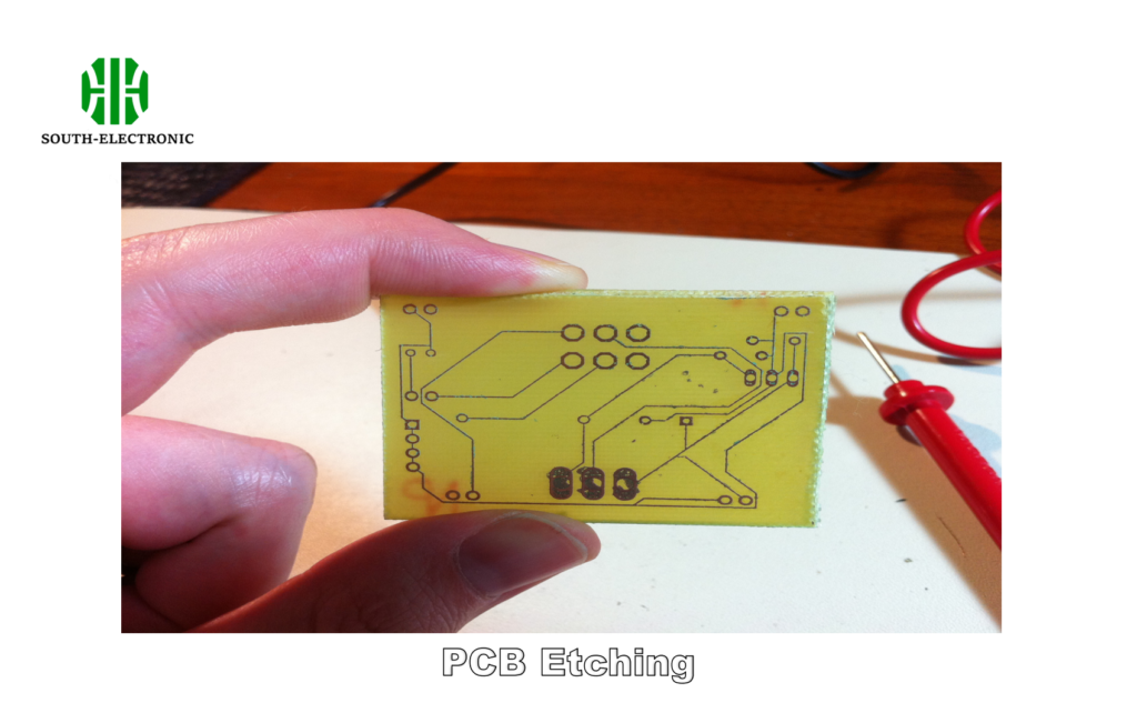
Ever ruined a PCB prototype because of messy copper traces? It costs time and money. Chemical etching solves this by removing unwanted copper precisely.
PCB chemical etching removes excess copper from boards using chemicals. A protective resist layer shields desired circuit patterns. The etchant dissolves exposed copper, creating clean conductive paths. This method efficiently forms intricate circuits.
This method shapes modern electronics. But what materials work best with it? How do we achieve accuracy? What tradeoffs exist? Let’s examine key aspects of chemical etching.
Which Materials Can Be Chemically Etched for PCB Applications?
Tried etching incompatible materials? They corrode or fail mid-process. Wasted effort damages components. I’ve seen aluminum boards melt in etchants.
Copper is the primary etched material. Aluminum and nickel alloys work too. Fiberglass substrates like FR-4 withstand etchants when properly masked.
Material Selection Depends on Three Factors
PCB materials fall into three categories based on their behavior during etching.
| Material Type | Examples | Key Properties |
|---|---|---|
| Metals | Copper, aluminum, nickel alloys | Conduct electricity but must dissolve evenly |
| Substrates | FR-4, polyimide, ceramics | Resist chemicals but support circuits |
| Resists | Photoresist, tin plating | Protect desired patterns during etching |
Metal compatibility matters most. Copper sheets work best because they etch uniformly. I once built a sensor board using copper. The lines stayed sharp.
Substrates and resists also matter. Fiberglass handles chemical baths. Photoresist must stick firmly during etching. Flimsy masks lead to fuzzy edges.
Avoid incompatible materials. Cheap boards sometimes use low-grade steel. Etchants attack them unevenly. Stick with copper for reliable results.
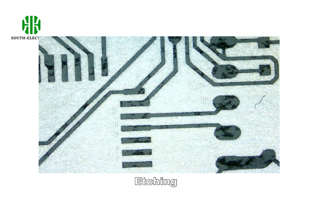
Achieving Precision in PCB Chemical Etching?
Frustrated by broken traces or short circuits? Imperfect etching causes malfunctioning hardware. Precise processes prevent costly errors.
Control etchant temperature and immersion time. Use automated spray systems. Monitor copper thickness with digital sensors regularly.
Precision Relies on Four Control Elements
We manage precision through these critical parameters:
Process Parameters
- Time: Longer exposure increases undercutting
- Temperature: Heat speeds etching but reduces control
- Agitation: Fluid movement ensures even results
Equipment Factors
| Tool | Function | Impact |
|---|---|---|
| Spray etchers | Direct chemical jets | Higher accuracy than dip tanks |
| Density meters | Track solution strength | Prevent over-etching |
| Temp controllers | Maintain bath heat | Consistent copper removal |
Undercutting is the enemy. It widens gaps between traces. I counter this with fresh chemicals and timed dips.
Measurement tools help. Digital timers prevent over-etching. Use them every batch. Skipped checks risk scrapping boards.
What Are the Key Pros & Cons of PCB Chemical Etching?
Choosing the wrong fabrication method? Errors multiply costs quickly. Know these tradeoffs to decide wisely.
Pros: Cheap for bulk production, highly detailed results, wide material options. Cons: Chemical hazards, copper waste, requires disposal systems.

Balanced View of Chemical Etching
Chemical etching offers both solutions and challenges:
Advantages
- Cost efficiency – Makes 50+ boards cheaper per unit than milling
- Complex designs – Creates traces under 0.005 inches wide
- Speed – Processes multiple boards simultaneously
Disadvantages
| Challenge | Impact | Mitigation |
|---|---|---|
| Toxic waste | Environmental harm | Neutralization tanks & certified disposal |
| Material loss | Up to 70% copper wasted | Copper recovery systems |
| Safety risks | Chemical burns | Protective gear & ventilation |
Waste disposal concerns me most. I installed filtration systems to handle used ferric chloride. This minimized environmental impact.
Precision demands control. For prototyping, I sometimes prefer mechanical methods. But mass production needs etching’s economies.
Conclusion
Chemical etching removes excess copper from PCBs using chemicals. It enables detailed circuits but requires safety measures. Understand materials and precision to use it well.

