
Ever designed a PCB only to face signal chaos? High-frequency errors can destroy your project. Avoid frustration by mastering these thresholds first.
High-frequency PCBs typically operate at 500 MHz or higher, though definitions vary. Fast digital signal edges may also require HF techniques even below 500 MHz. Material choice critically impacts what frequencies demand special design considerations.
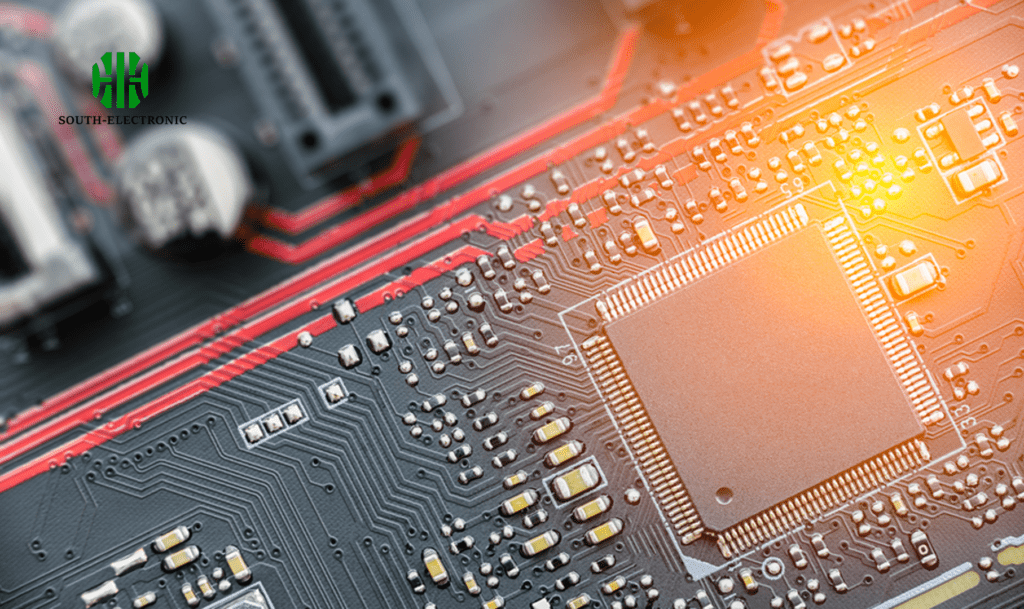
Understanding these ranges matters. But why? Let me explain how HF design changes everything for your boards.
Why Do High Speed Signals Need Special PCBs?
Signal distortion haunts fast circuits. Your data gets corrupted. That’s why unique PCB designs become essential.
High-speed signals suffer from reflections, crosstalk, and timing issues without proper impedance control. Specialized materials and layouts maintain signal clarity at high frequencies.
Core PCB Challenges at High Frequency
High frequency reveals hidden problems through three key effects:
-
Skin Effect
Current flows only on a conductor’s outer layer. This increases resistance drastically above 100 MHz. -
Dielectric Losses
Energy gets absorbed by the board material itself. Common FR4 resin acts like a signal sponge. -
Signal Reflections
Impedance mismatches make signals bounce unpredictably. Vias become mirrors.
| Frequency Range | Primary Threat | Mitigation Strategy |
|---|---|---|
| 100-500 MHz | Skin Effect | Wider traces |
| 500 MHz – 1 GHz | Dielectric Loss | Low-Df Materials |
| 1+ GHz | Reflections | Impedance matching |
I recall a WiFi module failing at 800 MHz due to untreated reflections. We fixed it with tapered microstrip lines and Teflon-based substrates. Material choice proved critical.
Why Can’t FR4 Handle Most High Frequency Applications?
FR4 seems reliable until signals accelerate. Then unexpected losses strike. Your design performance plummets without warning.
FR4’s inconsistent dielectric properties cause severe signal attenuation above 500 MHz. Its high dissipation factor (Df ~0.02) makes it unsuitable for most GHz applications.

The Material Limitations Breakdown
FR4 fails at high frequency for three structural reasons:
-
Resin Inconsistency
Woven glass fibers create uneven dielectric constants (Dk variance >10%). Signals encounter invisible speed bumps. -
Moisture Absorption
Trapped water increases loss exponentially. One humid week degrades performance. -
Thermal Instability
Dk values shift during operation. Your 50Ω trace becomes 47Ω when warm.
| Property | Standard FR4 | HF Material (e.g., Rogers) |
|---|---|---|
| Dissipation Factor | 0.018-0.025 | 0.001-0.005 |
| Dk Tolerance | ±10% | ±2% |
| Frequency Stability | Poor | Excellent |
During a 2.4 GHz project, our FR4 prototype lost 40% signal strength. Switching to Rogers 4350B solved it immediately.
Why is Lamination Control Critical for HF Multilayer Boards?
Laminate flaws hide between layers. Unexpected impedance drops appear. Your complex board fails final testing.
Precise lamination maintains uniform dielectric constant across layers. This ensures consistent impedance in stripline configurations critical for GHz signals.
Lamination’s Impact on Signal Quality
Three lamination factors determine HF success:
-
Resin Flow Control
Uneven resin creates thickness variations. Even 5% deviation changes impedance. -
Layer Alignment Accuracy
Misaligned cores distort electromagnetic fields. Signals leak between layers. -
Void Elimination
Air pockets alter dielectric constants locally. Each bubble acts like a signal prism.
| Defect Type | Frequency Impact | Detection Method |
|---|---|---|
| Thickness Variation | ±3Ω impedance shift | TDR measurements |
| Misalignment | Crosstalk increase | Impedance mapping |
| Resin Voids | Signal reflection | X-ray inspection |
I once saw a 16-layer board scrapped because resin voids caused GHz resonance. The manufacturer switched to vacuum lamination.
Does the Manufacturer Truly Specialize in High Frequency Production?
Many claim HF expertise. Few deliver. Hidden process gaps ruin boards. Testing reveals who’s qualified.
Truly experienced manufacturers use RF-specific processes: ceramic-filled laminates, laser ablation, and TDR validation. This prevents common failures that standard shops overlook.
Key Specialization Indicators
Evaluate manufacturers using these critical aspects:
-
Material Certification
Verified documentation for Dk/Df at your frequencies. Generic specs won’t suffice. -
Impedance Testing Methods
100% impedance verification via TDR proves reliability. Spot checks fail. -
Surface Treatment
Low-loss finishes like immersion silver. HASL creates impedance hills.
| Capability | Standard Shop | HF Specialist |
|---|---|---|
| TDR Testing | Sample basis | 100% testing |
| Dielectric Testing | Room temp | -40°C to 150°C |
| Tolerance | ±10% | ±2% |
One client discovered impedance variations with a new vendor. Third-party TDR testing showed 8Ω deviations they blamed on "normal tolerances."
Conclusion
High frequency PCBs start around 500 MHz but require special materials above 1 GHz. Proper design, manufacturing, and verification prevent costly signal disasters.

