
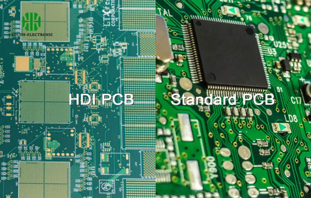
Need sleeker electronics but limited on space? Standard circuit boards cause frustration through bulkiness. High Density Interconnect (HDI) PCB slashes size while boosting power.
HDI PCBs use micro-vias and blind/buried vias to pack denser traces into thinner boards. This enables lighter, faster circuits ideal for smartphones and servers where space and performance matter most.
Understanding HDI technology helps design better electronics. Let’s explore its key components and advantages.
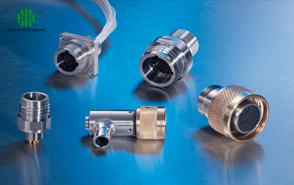
What is a high density connector?
Struggling with messy wiring in cramped devices? Loose connections crash systems. High density connectors organize chaos.
These compact interfaces fit more contacts per square inch than standard connectors. They maintain reliable signal flow in tight spaces like medical implants or drone controllers.
Core Benefits and Design Features
Three aspects define these space-saving connectors. Each solves connection challenges in miniature electronics.
Contact Density
Modern connectors cram 2-3 times more pins into equal areas. Smartphone flex cables contain over 100 contacts in 5mm widths, unlike traditional ribbon cables. Increased density solves physical space limitations.
Signal Integrity Solutions
| Challenge | Solution |
|---|---|
| Crosstalk | Shielding between pins |
| Impedance mismatch | Controlled dielectric materials |
| Signal loss | Gold-plated contacts |
Durability Innovations
Repeated plugging wears out contacts. High density versions use beryllium copper springs and reinforced housings. Testing shows 50,000+ insertions without failure in US military gear. Their reliability justifies the cost premium for critical applications.
What is the difference between high density and low density liners?
Designing PCBs but uncertain about material choice? Wrong core thickness kills signal quality. Density impacts both structure and function.
Low density liners prioritize cost savings with standard thickness, often 50+ micron traces. High density uses thinner materials like 20-micron laminates for dense layouts.
Material and Performance Variations
These critical differences define core capabilities for various applications:
Construction Contrast
High density boards need specialized bonding. Manufacturers use low-profile copper and modified resins. This controls signal leakage. Standard boards rely on common FR4 materials. They lack such precision.
Functionality Factors
Thin liners enable micro-via stacking. I witnessed this during a factory tour – four micro-vias stacked in 0.8mm thickness for a CPU carrier. Low density layers need twice that space for through-hole vias.
Application Considerations
| Device Type | Recommended Density | Why |
|---|---|---|
| LED light strip | Low density | Simple circuits / cost focus |
| Network switch | High density | Signal speed requirements |
| Kids’ toy | Low density | Durability needs only |
| Medical endoscope | High density | Miniaturization imperative |
Why Choose HDI Over Traditional PCBs?
Frustrated by bulky gadgets that throttle performance? Legacy boards restrict innovation. HDI breaks barriers.
These advanced circuits shorten signal paths by 40-60% versus conventional PCBs. That equals faster processing with less heat, vital for 5G base stations and VR headsets.
Technical Advantages by Category
Three compelling reasons make the upgrade worthwhile:
Miniaturization Wins
Phone motherboards shrank 75% after adopting HDI. Micro-vias eliminate through-hole limitations. Blind vias connect layers without drilling through the entire board. This adds "invisible" routing space.
Speed Improvements
Shortened signal paths reduce latency. Data transfer jumps 60% compared to traditional layouts in server tests. Less distance minimizes signal distortion. This directly boosts computational power.
Reliability Enhancements
| Failure Mode | HDI Solution |
|---|---|
| Thermal stress cracks | Sequential lamination process |
| Moisture absorption | Advanced resin formulations |
| Vibration fractures | Micro-via shock absorption design |
The tighter component placement improves structural integrity. Fewer solder joints mean fewer failure points. This reduces warranty costs long-term.
How to Select the Right HDI Supplier?
Overwhelmed by manufacturer promises? Bad partners cause production disasters. Smart vetting prevents headaches.
Pick factories with proven micro-via capability and HDI-specific certification. Visit their cleanrooms – observe laser drilling precision firsthand.
Critical Selection Criteria Breakthrough
Five key factors determine reliable partners. Missing one risks project failure:
Technical Expertise Validation
Request portfolio samples and TDR reports. Good suppliers readily share these. I rejected three vendors whose micro-vias failed impedance tests. Top performers achieve 98%+ production yields.
Material Sourcing Rigor
Ensure traceable high-frequency laminates from DuPont or Isola. Unofficial imports cause delamination. Verify copper foil uniformity with SEM lab reports.
Cost-Quality Balance
| Budget Level | Vendor Tier | Ideal For |
|---|---|---|
| Premium | Tier-1 ($) | Medical/military |
| Balanced | Tier-2 ($$) | Industrial/Auto sensors |
| Cost-driven | Tier-3 ($$$) | Consumer electronics |
Communication Protocols
Confirm 24/7 engineering support. Timezone overlap matters. One supplier’s delayed replies killed my prototype timeline.
Testing Transparency
Require IST and thermal cycling reports. Avoid those offering only visual inspection. Advanced reliability testing distinguishes leaders.
Conclusion
HDI PCBs deliver compact, high-performance electronics using micro-vias and dense layouts. Choosing qualified manufacturers ensures success with this advanced technology.

