
Ever struggled with weak circuit boards that crack under pressure? I’ve seen projects fail when cheap materials buckle. PCB laminates are your armor against chaos.
A PCB laminate forms the core structure of circuit boards, combining copper conductors with insulating materials like fiberglass and epoxy resin. I use them daily to create stable platforms for electronics, ensuring circuits stay separated and functional.
Knowing what laminates do is just the start. To truly master PCB design, we need to explore their key traits, pitfalls, and material differences next.
Which PCB laminate properties matter most for high-speed design?
Frustrated by ghost signals in your high-speed projects? I’ve wasted weeks debugging erratic circuits. Select laminates like a pro to avoid this nightmare.
Dielectric constant stability and low signal loss matter most for high-speed designs. I prioritize Dk consistency to prevent timing errors and focus on dissipation factor to maintain signal integrity above 5GHz.
When signals race faster than 1Gb/s, every laminate flaw magnifies. Three key properties separate winners from failures:
Performance Breakdown Table
| Property | Why It Matters | Ideal Value Range |
|---|---|---|
| Dk (Dielectric Constant) | Controls signal speed consistency | ±0.05 tolerance |
| Df (Loss Tangent) | Reduces signal energy loss | <0.005 @ 10GHz |
| CTE (Expansion Rate) | Prevents copper separation | <70ppm/°C |
Dk consistency keeps signals synchronized across long traces. A 5% variation causes clock skews ruining DDR5 designs. Low Df preserves signal strength: at 10GHz, a 0.01 Df sucks away 30% more power than 0.003 alternatives. CTE mismatches are silent killers – I've fixed boards where copper peeled off after thermal cycling because laminates expanded twice as fast as copper. Always verify manufacturer charts showing these values across your operating frequencies.
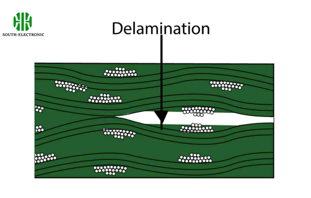
What are the defects of PCB lamination?
Burned by unexpected circuit failures? Last month, moisture-ruined laminates cost me $5k in scrap boards. Understand defects to save your designs.
Common defects I battle include delamination (layer separation), voids (air pockets), and resin starvation (weak bonds). Each causes catastrophic failures like short circuits or broken traces under stress.

Half of my production issues trace back to lamination flaws. They hide during testing but surface later:
Root Causes and Fixes
| Defect Type | Main Causes | Prevention Tricks |
|---|---|---|
| Delamination | Moisture absorption | Bake materials at 120°C |
| Voids | Trapped air during pressing | Vacuum lamination |
| Resin Starve | Incorrect pressure/temp | Follow material specs |
Delamination strikes hardest in humid climates – I add drying cycles before assembly now. Voids often originate from uneven prepreg stacking; using vacuum chambers eliminated 90% of mine. Resin starvation caused my worst field failure: a medical device cracked because we ignored manufacturer's pressure guidelines. Always cross-section test samples before full production runs.
What is the difference between prepreg and laminate PCB?
Confused about when to use core vs. prepreg? I once wasted materials mixing them up. Clear separation prevents costly errors.
Laminate PCBs are rigid finished cores with cured resin, while prepreg is uncured bonding material. I use cores as base structures and prepreg as glue between layers during lamination.

Their distinct roles shape multilayer boards. Consider them puzzle pieces:
Functional Comparison
| Characteristic | Laminate (Core) | Prepreg |
|---|---|---|
| State | Solid rigid sheet | Flexible uncured adhesive |
| Use Case | Structural foundation | Interlayer bonding |
| Handling | Direct circuit printing | Stacks between cores |
Cores provide stability – I select thickness based on stiffness needs. Prepreg's stickiness makes multilayer boards possible; its flow during heating fills gaps but requires precise temperature control. In 8-layer boards, I alternate 3 cores with 4 prepreg layers. Never use prepreg alone – it lacks structural integrity without core support. Store prepreg refrigerated to prevent premature curing.
Conclusion
PCB laminates dictate project success. Master their properties, avoid defects, and distinguish materials to build reliable, high-speed electronics efficiently.

