

Ever wasted weeks debugging a PCB only to find a wrong connection? A PCB netlist prevents that nightmare by acting as the circuit’s DNA. Let me explain why this unassuming text file is your design’s foundation.
A PCB netlist is an ASCII text file defining electrical connections between component pins. It bridges schematics and physical layout while enabling simulations and automated error checking – making it the single source of truth for PCB functionality.
While understanding netlists seems technical, mastering their role can prevent catastrophic design errors. Let’s break down how they work across different systems and stages.
How Do EDA Tools Generate a Netlist?
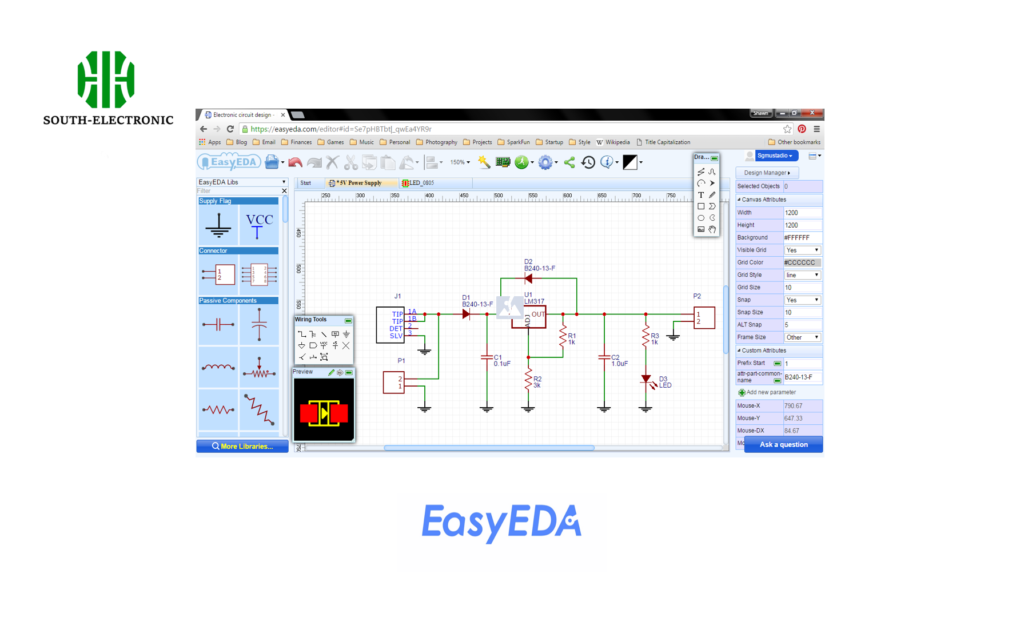
Watch your schematic transform into machine-readable instructions. EDA tools generate netlists by interpreting your drawings as mathematical connections – but not all tools do this equally.
EDA software like Altium Designer creates netlists by analyzing component pins and wires in schematics. Modern tools add metadata like net classes and differential pairs for layout guidance.
The Netlist Generation Process
Most tools follow three steps:
| Step | Action | Critical Checkpoints |
|---|---|---|
| 1. Schematic Parsing | Reads component symbols and wire connections | Verifies symbol pin counts match footprints |
| 2. Electrical Rule Validation | Checks for shorts/open nets | Flags unconnected power pins |
| 3. Format Exporting | Saves as SPICE/EDIF/other formats | Confirms compatibility with target layout tool |
The key is consistency. Last month, my colleague’s PCB failed because his EDA tool used lowercase "gnd" while the layout expected "GND". Always check net name capitalization early.
Why Is Netlist Verification Critical Before PCB Layout?
Skipping netlist checks is like building without blueprints. 63% of post-layout errors trace back to unverified netlists according to IEEE studies.
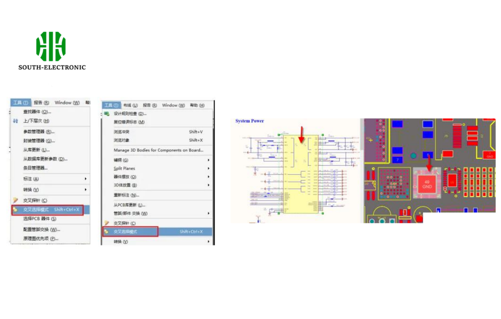
Netlist verification compares schematic connections with the generated file and target rules. It catches mismatches like swapped pins or missing components before costly production.

Common Verification Focus Areas
Create a checklist matching these priorities:
| Check Type | Tools Used | Critical Errors Detected |
|---|---|---|
| Electrical | SPICE, HyperLynx | Short circuits, floating nodes |
| Logical | FormalCheck, custom scripts | Signal direction mismatches |
| Physical | CAD Compare, DIFF | Footprint pin count mismatches |
I once saw a $25k prototype scrap because a DDR4 data line connected to a wrong bank – caught instantly in netlist checks but invisible in schematics. Verify thrice, prototype once.
SPICE vs EDIF Netlist: Which Format Fits Your Project?
Choosing the wrong format is like speaking French in Tokyo. SPICE and EDIF netlists serve different masters – know which one your tools understand.
Use SPICE netlists (.cir) for circuit simulation and analog analysis. Choose EDIF (.edf) for PCB layout and digital system integration.
Format Comparison Guide
| Factor | SPICE | EDIF |
|---|---|---|
| Best For | Simulations | Multi-tool Collaboration |
| Data Types | Analog Params | Hierarchical Design Data |
| Tool Support | LTspice, PSpice | Cadence Allegro, Altium |
| Readability | Human-friendly | Machine-optimized |
When designing a mixed-signal IoT board last year, I used SPICE for sensor validation and EDIF for layout – proving hybrids need both formats. Match the format to your current phase.
7 Netlist Errors That Could Ruin Your PCB Prototype
Ever seen a $10 typo kill a $10k board? These silent netlist killers slip past basic checks.
Top fatal netlist errors include swapped differential pairs, duplicate net names, missing power nets, incorrect pin mapping, unconnected chip enables, symbol-footprint mismatches, and unescaped special characters.
Error Prevention Checklist
| Error Type | Detection Method | Prevention Tip |
|---|---|---|
| Pin Swaps | Compare against datasheets | Highlight critical nets in schematics |
| Missing Nets | Cross-probing tools | Use ERC with strict rules |
| Name Clashes | Unique net labeling | Adopt "_" naming |
A missing underscore in "3V3_Audio" vs "3V3Audio" once merged power rails, frying op-amps. Never underestimate naming conventions.
Conclusion
PCB netlists transform abstract circuits into buildable blueprints. By choosing the right formats, running thorough verifications, and hunting sneaky errors, you’ll turn this technical step into your reliability secret weapon.

