
Are you tired of circuit boards failing due to poor connections? Plated through hole technology solves this headache. It ensures signals travel reliably across your PCB layers.
Plated through holes are copper-lined holes drilled through PCBs. They create electrical pathways between layers while strengthening component mounts. This core PCB feature enables complex circuitry in electronics.
Understanding PTH is crucial for electronics work. Let me break down key questions I often get from engineers.
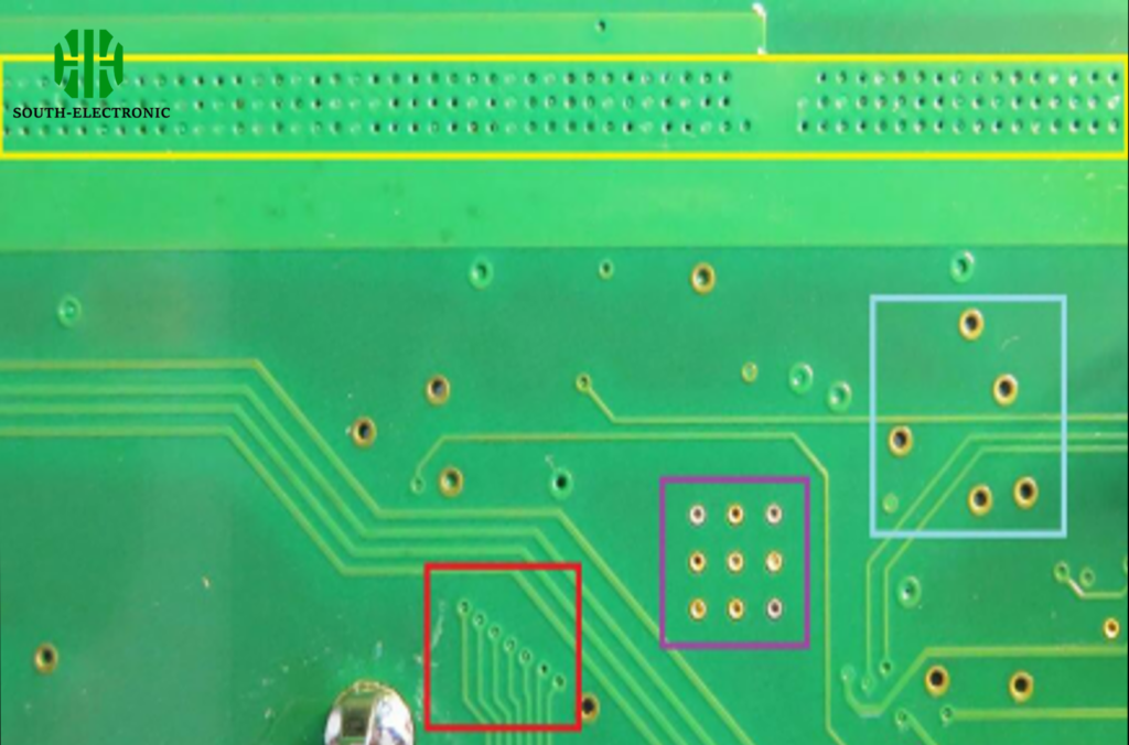
How is PTH different from a non-plated through hole (NPTH)?
Do NPTHs cause unexpected disconnections in your projects? Non-plated holes create mechanical weaknesses without conductivity benefits.
Unlike NPTH, plated through holes have conductive copper barrel lining. PTH transfers electricity across layers while NPTH serves only physical mounting needs. Choose PTH for electrical connections.
Electrical and functional differences
These hole types serve fundamentally different purposes:
| Feature | Plated Through Hole | Non-Plated Through Hole |
|---|---|---|
| Conductivity | Copper lining enables current flow | No conductivity |
| Typical Use | Component leads & layer connections | Mounting screws/markers |
| Failure Risk | Barrel cracks affect signals | No electrical impact |
Plated through hole pcb design requires considering thermal stress during soldering. The copper lining expands differently than PCB material. NPTHs avoid this issue but cannot carry signals. I recall misplacing an NPTH in a power supply design – it caused frustrating debugging sessions. Always verify hole types before finalizing layouts.
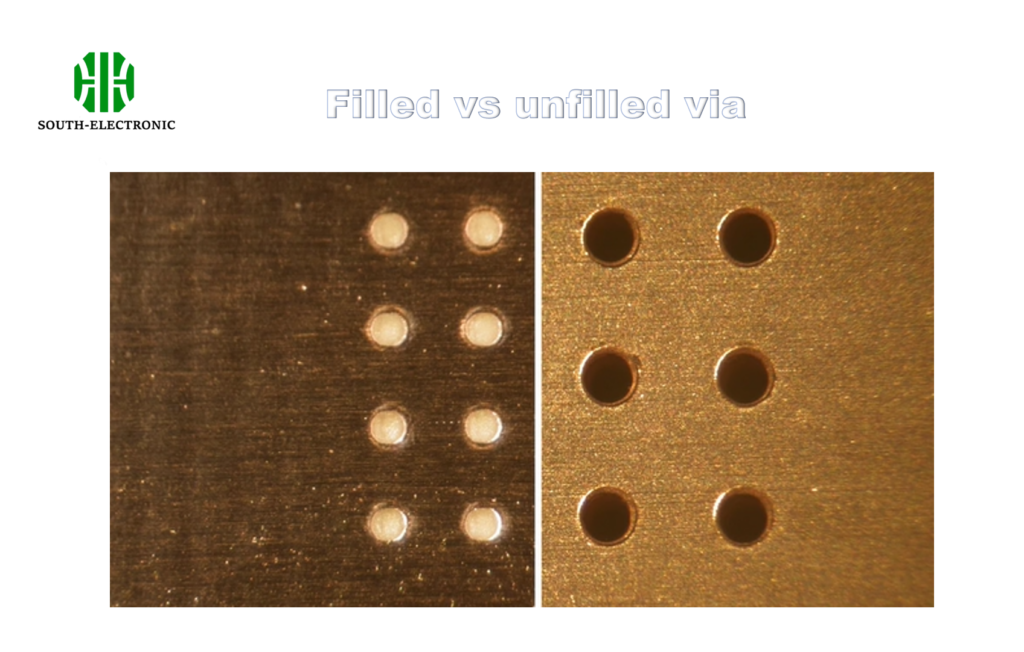
Are through-holes, blind vias, and buried vias all PTHs?
Confused why vias act differently in multi-layer boards? Not all hole-based connections share PTH properties.
Blind/buried vias are specialized plated holes but with partial penetration. Like standard PTH, all use copper plating for connectivity. Through-holes span entire boards while vias connect specific layers.
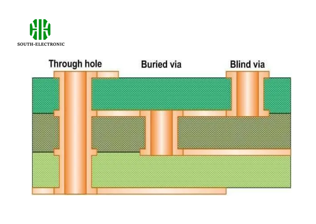
Structural distinctions and uses
Each connection type serves unique PCB layout needs:
| Type | Connection Range | Visibility | Plating Used? |
|---|---|---|---|
| Through-Hole | All layers | Full visible | Yes (PTH) |
| Blind Via | Surface-inner layer | One side only | Yes |
| Buried Via | Internal layers only | Not visible | Yes |
Through-hole plated through hole works for component leads spanning boards. Vias help route dense traces without surface clutter. In my RF projects, blind vias reduced interference remarkably. Remember: all share plating but differ dramatically in function and manufacturability. Double-layer boards typically use standard PTH exclusively.
How is PTH manufactured?
Ever wonder how copper gets inside microscopic PCB holes? Plated through hole technology transforms drilled holes into conductive pathways.
Manufacturing involves precise drilling followed by chemical copper deposition. First, hole walls absorb catalytic chemistry then undergo electroplating. Finally, tin protects copper barrels during etching.
Step-by-step production process
Creating reliable plated connections requires careful chemistry control:
| Stage | Process | Critical Factors |
|---|---|---|
| Hole Preparation | Mechanical laser drilling | Clean hole walls |
| Activation | Apply palladium catalyst | Even surface coverage |
| Copper Deposition | Electroless plating | Temperature/time control |
| Strengthening | Electroplating | Electrical current stability |
Drilling consistency impacts plated through hole reliability. Too fast creates barrel voids while slow drilling causes resin smear. I once saw poorly plated holes cause automotive module failures in cold weather. Testing finished boards must include cross-section analysis for copper uniformity. This technology remains fundamental despite newer PCB innovations.
Conclusion
Plated through holes form vital PCB connections via copper-lined holes. Their design and manufacturing require precision for reliable electronics operation.

