

Modern electronics demand creative solutions for cramped spaces. Rectangular circuit boards often leave unused gaps in circular products. Round PCBs solve this problem by perfectly fitting devices requiring compact, space-efficient layouts.
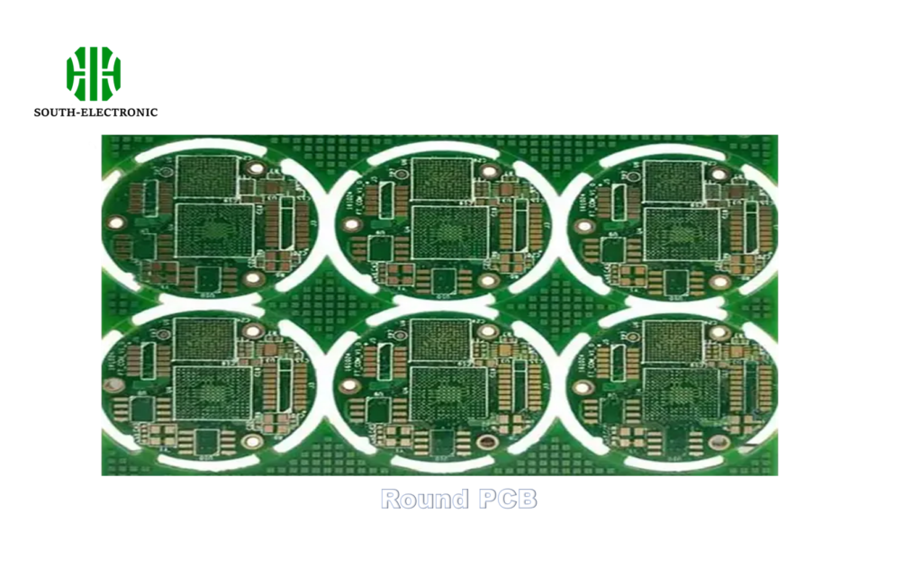
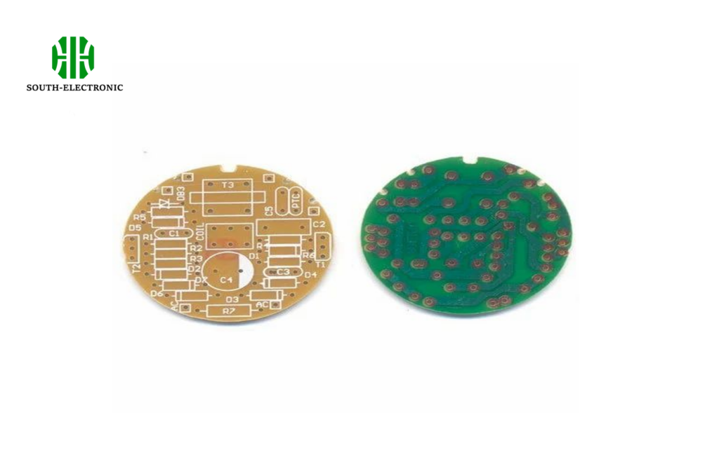
Round printed circuit boards[^1] feature circular shapes for specialized devices like wearables and IoT gadgets. Unlike angular boards, they optimize space usage and simplify mechanical integration while maintaining standard electrical functions.
While round PCBs offer clear advantages, their unique geometry creates distinct design and production challenges. Let’s explore what makes these circular boards stand out and how to work with them effectively.
What Makes Round PCBs Different From Traditional Circuit Boards?
Designers accustomed to right-angle layouts hit roadblocks when components resist circular arrangements. Rotation angles and component spacing become critical variables in round designs.
Key differences include radial component placement[^2], curved trace routing, and specialized manufacturing processes. These circular boards require precise calculations for heat distribution and signal integrity compared to rectangular boards.
Three Critical Design Divergences
-
Component Orientation Challenges
- Radial symmetry requires 360-degree placement planning
- Automated assembly adapters need custom calibration
| Feature | Rectangular PCB | Round PCB |
|---|---|---|
| Trace paths | Straight lines | Curved arcs |
| Ground planes | Uniform | Segmented wedges |
| Impedance control | Predictable | Varies by radius |
- Manufacturing Adjustments
Panel utilization drops from 90% to 70% due to circular board waste
Laser drilling often replaces mechanical drills for precise edge shaping
How to Avoid Common Mistakes in Round PCB Design?
Engineers new to circular layouts frequently underestimate mechanical stress points. A fitness tracker PCB failed during testing because traces cracked at the 12 o’clock position.
Always reinforce high-stress zones[^4] with thicker copper weights. Use teardrop-shaped pad connections and avoid 90-degree trace angles near the board edge.
Essential Design Safeguards
-
Circular Routing Rules
- Maintain minimum 0.5mm clearance between traces and board edge
- Implement curved instead of angular trace corners
-
Component Placement Protocol
| Component Type | Ideal Placement Zone | Risk Zone |
|---|---|---|
| Large capacitors | Central area | Outer third |
| Fine-pitch ICs | North/South quadrants | East/West edges |
| Connectors | Pre-cut notch locations | Random edge placements |
- Thermal Expansion Planning
Radial expansion differs from rectangular boards – coefficient calculations must account for 360-degree stress distribution. Use ANSYS simulations for high-temperature applications.
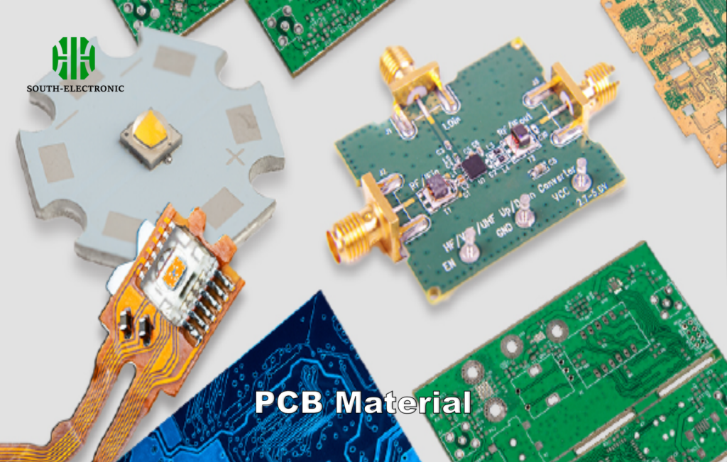
What Material Considerations Matter Most for Circular Board Performance?
Standard FR4 behaves differently when cut into circles. A medical implant PCB warped because the material couldn’t handle radial shrinkage during soldering.
Prioritize materials with balanced CTE (Coefficient of Thermal Expansion[^5]) across all axes. Flexible substrates like polyimide often outperform rigid boards in curved applications.
Material Selection Matrix
- Core Material Options
| Material | Flexibility | Thermal Tolerance | Cost |
|---|---|---|---|
| FR4 | Rigid | 130°C | $ |
| Polyimide | Flexible | 260°C | $$$ |
| Aluminum | Semi-rigid | 150°C | $$ |
-
Conductive Layer Requirements
- 2-oz copper recommended for outer layers to resist peeling
- Electroless nickel coating prevents edge oxidation
-
Specialized Finishes
Use ENIG (Electroless Nickel Immersion Gold) for edge connectors subjected to frequent friction
Avoid HASL (Hot Air Solder Leveling) for boards with components within 1mm of edge
How Do Manufacturers Ensure Quality in Curved Edge PCB Production?
A batch of smartwatch PCBs failed because the beveled edges caused registration errors during assembly. This cost $28,000 in rework labor.
Advanced optical inspection systems[^6] map component positions based on polar coordinates instead of Cartesian grids. X-ray tomography[^7] checks layer alignment within 5μm tolerance.
Precision Manufacturing Techniques
- Cutting Method Comparison
| Technique | Edge Precision | Material Waste | Speed |
|---|---|---|---|
| Laser Cutting | ±0.01mm | 5% | Slow |
| Punch Press | ±0.1mm | 18% | Fast |
| CNC Routing | ±0.05mm | 12% | Moderate |
-
Layer Registration Systems
- Use fiducial markers at 120° intervals
- Implement automated θ-axis compensation
-
Testing Protocol Enhancements
Flying probe tests follow spiral patterns instead of linear sweeps
Thermal cycling tests include rotational stress simulations
Conclusion
Round PCBs enable compact, efficient device designs but demand specialized engineering approaches. Proper material choices, stress-aware layouts, and precise manufacturing ensure reliable performance in circular electronics applications.
[^1]: Discover the advantages of round PCBs for compact designs and their impact on modern electronics.
[^2]: Learn about the unique challenges and strategies for effective radial component placement in circular designs.
[^3]: Explore the intricacies of signal routing in round PCBs and how it differs from traditional layouts.
[^4]: Understanding high-stress zones is crucial for ensuring the durability and reliability of your PCB designs. Explore this resource to learn more.
[^5]: The Coefficient of Thermal Expansion is vital for material selection in PCBs. This link will provide deeper insights into its importance and applications.
[^6]: Explore how advanced optical inspection systems enhance PCB quality and precision, ensuring reliable performance in electronics.
[^7]: Learn about X-ray tomography’s role in achieving precise layer alignment in PCBs, crucial for high-quality manufacturing.

