
Solder paste can cause short circuits. Tired of unexpected electrical glitches? Solder mask protects your circuits from these issues, ensuring reliable performance.
A solder mask[^1], also called solder resist, is a protective layer applied to printed circuit boards[^2] (PCBs). It insulates copper traces and prevents solder bridges[^3] during assembly, which stops short circuits and improves board durability.
You might wonder how this thin layer makes such a big difference in electronics. Understanding its role is key to building robust devices. Let's explore why solder mask is essential.
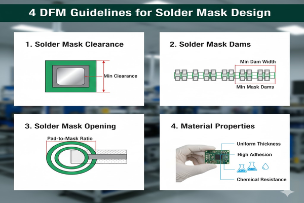
What are 4 DFM Guidelines for Solder Mask Design?
Struggling with PCB manufacturing failures[^4]? Poor solder mask design is often the culprit. Proper design prevents costly rework and ensures successful production.
Four key Design for Manufacturability (DFM) guidelines for solder mask are ensuring proper clearance, adequate solder mask dam size, correct pad definition[^5], and consideration of material properties[^6]. Following these helps avoid manufacturing problems.
When I first started designing PCBs, I overlooked the importance of solder mask design. This led to frustrating issues like solder bridging and components not sitting properly. Now, I always follow these guidelines to make sure my boards are reliable.
Solder Mask Clearance
Solder mask clearance is the space between the solder mask opening and the copper pad.
- Too small: Solder mask can encroach on the pad, causing issues like tombstoning or poor solder joints.
- Too large: Exposed copper traces can lead to solder bridging.
- Standard: Typically 2-4 mil (0.05-0.1 mm) around the pad.
Solder Mask Dam
A solder mask dam is the strip of solder mask material between adjacent pads.
- Purpose: Prevents solder from flowing between pads, especially on fine-pitch components.
- Minimum Width: Generally 4 mil (0.1 mm) or more. Smaller dams can lift or break during manufacturing.
Pad Definition
This refers to how the solder mask opening relates to the copper pad.
- Non-Solder Mask Defined (NSMD): Solder mask opening is larger than the copper pad. This exposes a ring of copper, leading to better solder joint reliability[^7] for some components.
- Solder Mask Defined (SMD): Solder mask opening is smaller than the copper pad. The solder mask defines the pad area. This can be useful for very fine-pitch components to prevent solder migration.
Material Properties
Different solder mask materials have varying thermal and chemical resistance.
- Consider: Operating temperature, chemical exposure, and desired durability.
- Impact: Affects adhesion, reliability, and lifespan of the PCB.
| Guideline | Description | Importance |
|---|---|---|
| Solder Mask Clearance | Space between mask opening and pad | Prevents solder encroachment/bridging |
| Solder Mask Dam | Mask strip between adjacent pads | Stops solder bridging on fine-pitch components |
| Pad Definition | How mask opening relates to copper pad | Affects solder joint reliability and formation |
| Material Properties | Thermal and chemical resistance of mask material | Impacts board durability and performance |
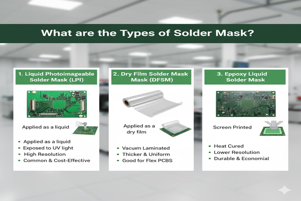
What are the Types of Solder Mask?
Confused by different solder mask colors and textures? Each type serves a specific purpose. Knowing the options helps you choose the best one for your project.
Solder masks come in various types, including Liquid Photoimageable Solder Mask[^8] (LPI), Dry Film Solder Mask[^9] (DFSM), and Epoxy Liquid Solder Mask[^10]. Each type offers distinct characteristics in terms of application, resolution, and cost, suitable for different PCB manufacturing needs.
When I was first learning about PCB fabrication, I thought solder mask was just "green stuff." But I soon learned that there's a whole world of options, each with its own benefits and drawbacks. Understanding these helps me make better design choices.
Liquid Photoimageable Solder Mask (LPI)
LPI is the most common type of solder mask today.
- Application: Applied as a liquid, then exposed to UV light through a phototool. Unexposed areas are washed away.
- Resolution: Offers high resolution, making it suitable for fine-pitch designs.
- Colors: Available in many colors like green, red, blue, white, black, and yellow.
- Cost: Cost-effective for high-volume production.
- Durability: Good adhesion and chemical resistance.
Dry Film Solder Mask (DFSM)
DFSM is a pre-formed sheet of solder mask material.
- Application: Laminated onto the PCB using heat and pressure, then exposed and developed.
- Resolution: Lower resolution compared to LPI, generally used for less dense boards.
- Thickness: Provides a more uniform thickness, which can be an advantage for some designs.
- Cost: Often more expensive than LPI for large-scale production.
Epoxy Liquid Solder Mask
This is a screen-printed solder mask.
- Application: Applied through a silk-screen process.
- Resolution: Lower resolution, mostly used for basic, less dense PCBs.
- Durability: Good electrical insulation and chemical resistance.
- Cost: Generally inexpensive.
| Solder Mask Type | Application Method | Resolution | Common Use Case | Key Feature |
|---|---|---|---|---|
| Liquid Photoimageable (LPI) | UV exposure[^11], development | High | Fine-pitch PCBs, high volume | Versatile, high precision |
| Dry Film (DFSM) | Lamination, development | Medium-Low | Less dense boards | Uniform thickness |
| Epoxy Liquid | Screen printing | Low | Basic PCBs | Cost-effective |
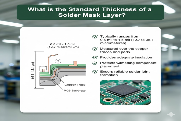
What is the Standard Thickness of a Solder Mask Layer?
Worried about your solder mask being too thin or thick? Incorrect thickness can lead to manufacturing issues and reliability problems. Knowing the standard helps ensure quality.
The standard thickness of a solder mask layer typically ranges from 0.5 mil to 1.5 mil (12.7 to 38.1 micrometers) over the copper traces and pads. This thickness provides adequate insulation and protection without impeding component placement or solder joint formation.
I remember a project where the solder mask was applied too thin. This caused exposed copper and subsequent short circuits. We had to rework many boards. Now, I always confirm the thickness specifications with the manufacturer to avoid such headaches.
Factors Influencing Thickness
Several factors dictate the optimal solder mask thickness.
- Copper Weight: Thicker copper traces often require a slightly thicker solder mask to ensure full coverage.
- Component Density: Denser boards with fine-pitch components might need precise thickness control to prevent bridging.
- Solder Mask Type: LPI masks generally offer more consistent thickness control than screen-printed epoxy masks.
- Application Method: The method used to apply the mask (e.g., spraying, curtain coating, screen printing) affects uniformity.
Measurement and Control
Ensuring correct thickness is a critical part of quality control.
- Microsectioning: Boards are cut and polished to visually inspect the thickness under a microscope.
- Non-Contact Methods: Optical measuring tools can provide accurate thickness readings without damaging the board.
- Importance: Consistent thickness ensures proper insulation, prevents solder migration, and maintains the integrity of the PCB.
| Aspect | Description | Impact on PCB |
|---|---|---|
| Over Copper Traces | Typically 0.5 to 1.5 mil (12.7 to 38.1 µm) | Ensures insulation and prevents shorts |
| Over Base Laminate | Can be thicker, 1.0 to 2.0 mil (25.4 to 50.8 µm) | Provides overall protection to the PCB surface |
| Uniformity | Critical for consistent performance | Prevents localized weak points or bridging |
| Measurement | Microsectioning, optical tools | Verifies quality and adherence to specifications |
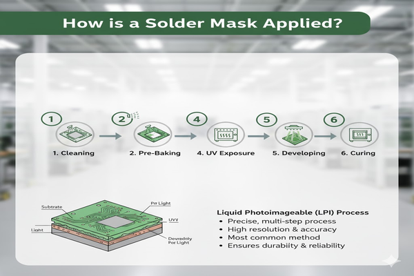
How is a Solder Mask Applied?
Curious about how that protective green layer gets onto your PCB? The application process is precise and crucial for board reliability. Let's break it down.
Solder mask is applied through several methods, most commonly liquid photoimageable (LPI) processes involving cleaning, coating, pre-baking, UV exposure, developing, and final curing. Each step is carefully controlled to ensure accurate coverage and adhesion, protecting the underlying copper traces.
I've watched PCBs go through the solder mask application process many times. It’s a fascinating sequence of steps that transforms a bare copper board into a protected circuit. The precision involved is truly impressive.
Step-by-Step LPI Process
The LPI process is widely used due to its high resolution and efficiency.
- Cleaning: The PCB surface is thoroughly cleaned to remove contaminants, ensuring good adhesion of the solder mask. This often involves chemical cleaning and scrubbing.
- Coating: The liquid photoimageable resist is applied to the entire surface of the PCB. This can be done by curtain coating, spray coating, or screen printing.
- Pre-Baking: A short bake removes solvents from the liquid resist, making it tacky but solid enough for the next step.
- UV Exposure: The PCB is exposed to UV light through a phototool (a film mask with the desired pattern). The areas exposed to UV light polymerize and harden.
- Developing: The unexposed (unhardened) areas of the solder mask are washed away using a chemical developer, revealing the copper pads where components will be soldered.
- Final Curing: The PCB undergoes a final thermal cure, typically in an oven, to fully harden and cross-link the solder mask, providing maximum durability and chemical resistance.
Other Application Methods
While LPI is dominant, other methods exist.
- Screen Printing: Used for epoxy liquid masks, involves pushing the liquid through a fine mesh screen to create the pattern. Lower resolution.
- Dry Film Lamination: Dry film sheets are laminated onto the board with heat and pressure, then exposed and developed like LPI.
| Application Method | Solder Mask Type | Resolution | Key Stages | Advantages |
|---|---|---|---|---|
| LPI Process | LPI | High | Cleaning, Coating, Pre-bake, UV, Develop, Cure | High precision, versatile, standard for modern PCBs |
| Screen Printing | Epoxy Liquid | Low | Cleaning, Printing, Curing | Cost-effective for simple designs |
| Dry Film Process | DFSM | Medium-Low | Cleaning, Lamination, UV, Develop, Cure | Uniform thickness, good for certain applications |
Conclusion
Solder mask is a vital protective layer for PCBs. It prevents shorts and improves reliability, making it indispensable for functional electronics.
[^1]: Explore the essential role of solder mask in ensuring reliable circuit performance. [^2]: Learn about PCB manufacturing processes to enhance your electronics knowledge. [^3]: Discover effective strategies to avoid solder bridges in your PCB designs. [^4]: Identifying failure causes can help you improve your PCB design and production. [^5]: Explore how pad definition affects solder joint reliability in your designs. [^6]: Understanding material properties can help you choose the right solder mask for your project. [^7]: Explore factors affecting solder joint reliability to enhance your designs. [^8]: Discover the benefits of LPI for high-resolution PCB designs. [^9]: Learn about DFSM's applications and advantages in PCB manufacturing. [^10]: Explore the features of epoxy masks for cost-effective PCB solutions. [^11]: Learn how UV exposure contributes to the effectiveness of solder masks.

