
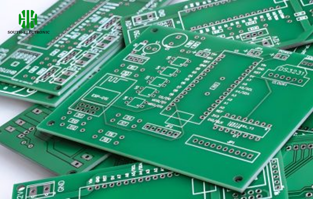
"A good detective can always detect details that seem completely inconspicuous. Small problems that go unnoticed by others may be clues to solving a mystery. Similarly, some holes in PCB design may seem insignificant, but without these "tooling holes", the board will not achieve the intended function or even be manufactured correctly."
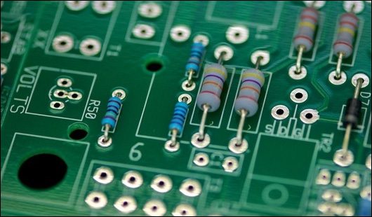
Individually, the tooling holes on the circuit board look ordinary because they are regular-looking through holes drilled on the circuit board. Only by carefully studying their role can we truly understand their importance.
Some of these through holes are used to connect hardware to the circuit board, while others are used to help the manufacture and assembly of the circuit board.
What is the role of PCB tooling holes?
In the design and manufacture of PCBs, many different sizes of holes are usually drilled on the board, and these holes will be suitable for different functions. Most holes are used to interconnect electrical signals between layers, and some holes are used to solder components and for mounting different hardware. Tooling holes (also called "mounting holes") used to connect hardware can be associated with the package pattern of the component or can be marked separately.
In addition to enabling leads or pins to be soldered to the board, some components also have mounting hardware for added physical support. Connectors are often bolted to the board to protect their soldered parts from the stress of plugging and unplugging cables. Other components that are heavier or used as interfaces may also be screwed on, including switches, fans, batteries, and speakers.
These holes may also be needed to connect mounting hardware to electrical grounds or conduct heat through the board to disperse on internal plane layers. Finally, in order to install the PCB into its system, isolation holes are often used to connect the hardware or brackets that need to be mounted to the board. PCB tooling holes can be placed on the board to facilitate the coordination of different manufacturing stages. These holes guide the board through its assembly process, such as reflow soldering, wave soldering, and automated optical inspection (AOI). If the PCB needs to undergo additional testing, the tooling holes are also used during the testing process.
What are the design standards for regular holes?
If tooling holes are required on the board during any manufacturing process, the manufacturer will require that they be added to the design.
Typically, the manufacturer will use holes that already exist on the board or add them to the manufacturing files. Holes are created for mounting hardware and must be machined with the correct design parameters to function as intended:
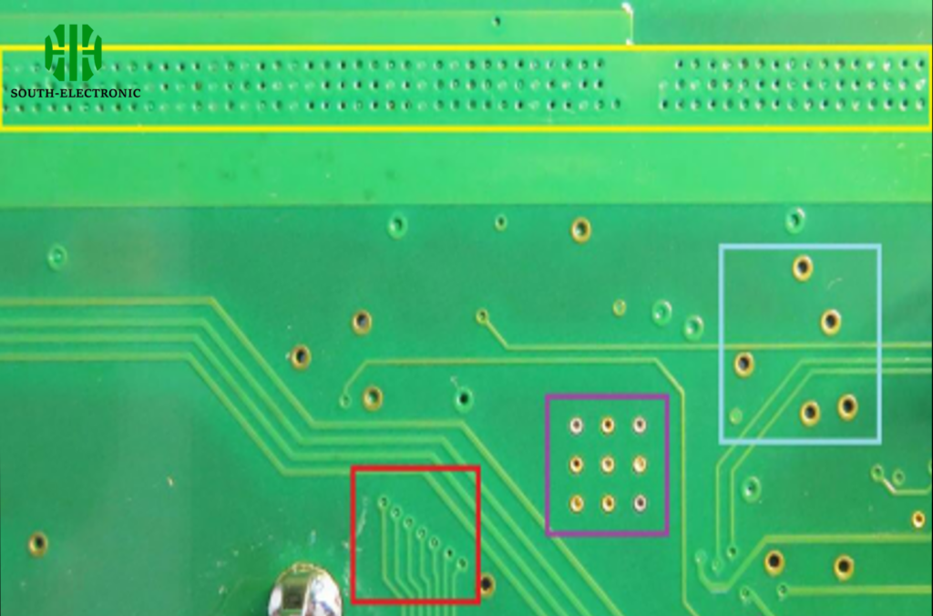
Location: The number of machined holes and their locations depend on the requirements of the board and component. Component datasheets typically specify the location of these holes, and designers should include this in their PCB footprint.
Preferred size: This again depends on the requirements of the component. Typically, these parts will use 4-40 or 6-32 screws and must be drilled to match the mounting hardware. If the design does not include system mounting holes, PCB manufacturers generally recommend adding some common 0.100 or 0.125 inch holes to facilitate subsequent mounting options.
Plating: This depends on the hardware requirements that need to be mounted. For hardware that needs to be electrically connected to the board, the holes must be plated and connected to the appropriate net, otherwise unplated holes should be used.
Plane connection: Plated holes connected to the power or ground plane must not be connected to any other plane to prevent shorting of the power and ground nets. Improperly designed mounting holes may eventually interfere with design rule checks.
Spacing: Holes that house mounting hardware often require large shielded areas around them. Mounting hardware needs enough space to securely contact the board without damaging component leads or metal traces and planes. Additional clearance around plated holes is also critical, and plated holes need to be drilled larger to allow the added plating material to finish the holes to the required size.
Although tooling holes and mounting holes may not seem to have much impact on PCB layout. In fact, the design and mounting holes need to pay the same attention to details as the PCB design process. There are also many factors in the design that are important for manufacturing.
What are the factors that affect manufacturing?
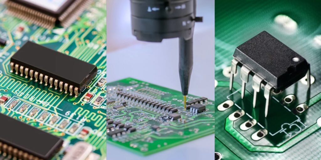
In addition to the different PCB tooling holes required for mounting hardware and production aids, there are also design issues that need to be paid attention to in the design that may affect PCB manufacturing. These include solder paste pads for surface mount component pins, solder mask to protect the board and silkscreen markings for component reference markings and corporate logos.
In addition, designers should also pay attention to the issue of fiducial pads. They are small pads used for PCB alignment during automated assembly. Fiducial pads are usually placed in the corners and center of large SMT devices with high pin counts.
It can be challenging for designers to meet all the requirements for PCB manufacturing and assembly. But that is exactly what a good PCB design engineer should do.

