

Traces on one layer just won’t cut it for complex circuits. Your design gets messy and crowded fast. Frustrating, right? Vias solve this by connecting layers cleanly.
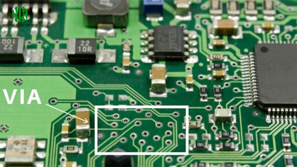
A via is a tiny conductive tunnel piercing through your PCB layers. It carries signals or power vertically, like an elevator between floors in a circuit skyscraper. Careful design prevents signal loss and overheating.
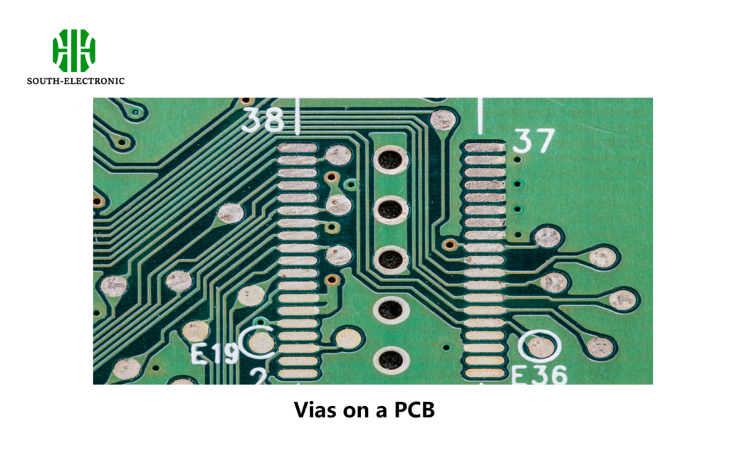
Vias transform flat layouts into 3D electrical highways. But choosing the wrong type can wreck your board. Let’s explore key via decisions that make or break designs.
When Should You Use Blind and Buried Vias in High-Density PCB Designs?
Packing components tight leaves zero extra space. Standard vias hog valuable real estate. Your delicate routing gets choked.
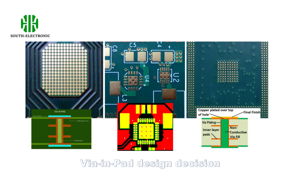
Blind and buried vias create hidden vertical tunnels. They link only specific internal layers, freeing up surface space for components. Ideal for smartphones or wearables battling space constraints.
Space vs Manufacturability Tradeoffs
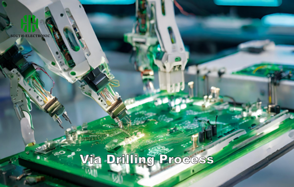
These specialized vias require laser drilling and precise plating. While costly, they enable impossibly dense boards. Three factors dictate their use:
| Factor | Blind Vias | Buried Vias |
|---|---|---|
| Layer access | Surface to inner layer | Inner-to-inner only |
| Visibility | Visible on one surface | Fully hidden |
| Cost impact | Moderate increase | High increase |
| Best for | Escape routing under BGAs | Complex multi-layer processors |
Blind variants start drilling from outer layers, stopping partway. They clear space under chips like microcontrollers. Buried types stay completely internal, preserving both surface layers. I once fried a prototype by cramming standard vias under a Wi-Fi module – learned this lesson the hard way!
Through-hole vias work for simpler boards, but modern tech demands sophistication. When component spacing drops below 0.5mm, these stealth connectors become mandatory. Remember: each additional lamination step raises costs 15-30%. Balance density needs against budget realities.
How to Calculate Optimal PCB Via Size and Spacing for Your Circuit Board?
Tiny vias overheat during power surges. Spaced too close, they create signal crosstalk. Your elegant schematic turns into smoking rubble.
Base dimensions on current needs and fabrication limits. Follow IPC-2221 standards for reliable manufacturing. Smaller vias save space but increase resistance and cost.
The Via Geometry Equation
Balancing current capacity against space efficiency requires math. Three parameters dominate:
| Parameter | Calculation Method | Risk of Ignoring |
|---|---|---|
| Diameter | Minimum = 8*(board thickness) | Drill breakage during fabrication |
| Current capacity | Use online pcb via current calculator | Melted conduits during operation |
| Pad spacing | >3x drill diameter | Short circuits during solder wicking |
Example: For 1A current, a standard 0.3mm via barely suffices. Pushing 3A demands 0.6mm or multiple vias. Always add thermal reliefs to pads – I’ve seen countless lifted traces without them.
Spacing depends partly on pcb via tenting preferences. Covered vias (tented) need less clearance than exposed ones. For impedance-sensitive lines, maintain at least 3x drill width between via pads. That 6-layer IoT controller board on your bench? Its 0.2mm micro-vias need military-grade precision.
Why Do PCB Vias Fail?
Plated walls develop cracks after temperature swings. Tiny voids trap moisture during soldering. Suddenly your flawless board develops dead zones – disastrous in mission-critical systems.
Thermal stress and chemical contamination cause 74% of failures. Manufacturing flaws like uneven plating create weak spots while poor hole drilling leaves ragged walls.
Three Silent Killers
Understanding failure mechanisms prevents debugging nightmares. Critical factors include:
- Material Stress: Different layer expansion rates during heating cycles. FR4 expands 13ppm/°C while copper expands 17ppm/°C – mismatch causes fatigue fractures
- Plating Weakness: Thin copper coatings (5A, stick with through-hole vias – their conductive mass handles heat better.
Beware reliability tradeoffs: complex micro-via stacks risk layer registration errors. And always specify copper-filled types (pcb via fill) when placing them under heatsinks. That gaming laptop’s thermal throttling issue? Traced to insufficiently filled GPU power vias.
Conclusion
Choose via types based on current, space and cost. Use micro-vias for modern miniaturization. Prevent failures with robust design rules. Every connection impacts your board’s success.

