

Our modern lives depend on seamless WiFi connectivity. But what makes this invisible connection work? Behind every smooth video call or buffer-free movie lies a hidden hero: the WiFi PCB.
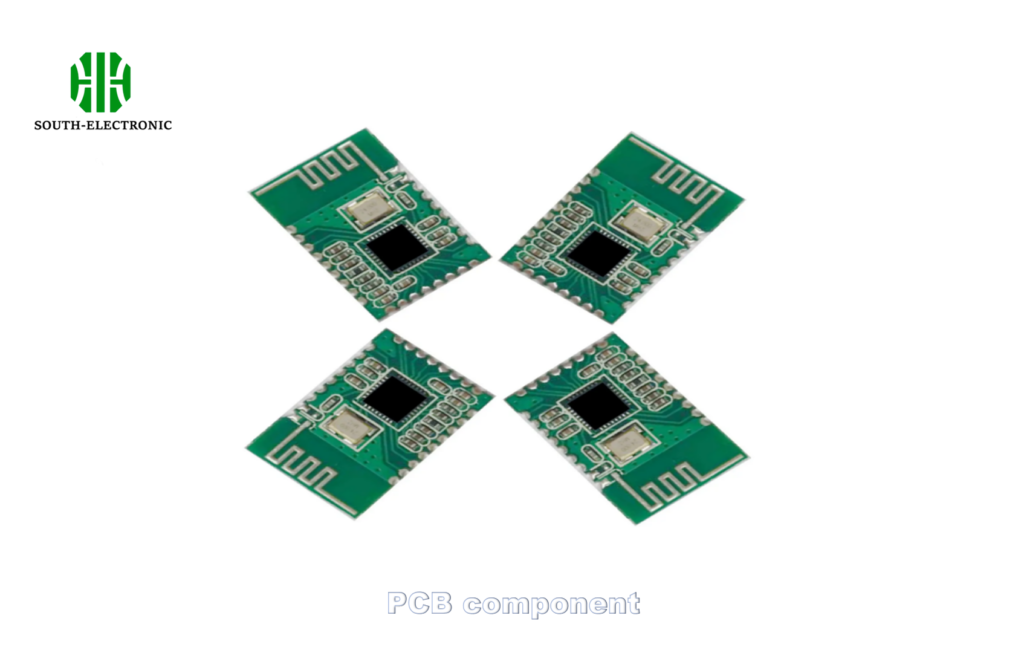
A WiFi PCB is a specialized circuit board designed to enable wireless communication through carefully integrated antennas, radio transceivers, and signal processing components that handle data transmission for 2.4GHz/5GHz frequencies.
Let’s dissect the four critical aspects of WiFi PCB design that determine whether your device becomes a connectivity champion or a frustrating paperweight.
What Core Components Make Up a WiFi PCB System?
Imagine downloading a crucial file when your WiFi suddenly drops. This nightmare scenario traces back to missing or flawed core components in the PCB’s wireless system.
Every WiFi PCB[^1] requires three essential elements: radio frequency transceivers[^2] for wireless data conversion, impedance-matched antenna structures[^3] for signal radiation, and power amplifiers/ filters to boost and clean signals before transmission.
Anatomy of Wireless Functionality
| Component | Role | Key Specifications |
|---|---|---|
| Antenna | Radiates WiFi signals | Gain, radiation pattern |
| RF Transceiver | Converts digital-RF signals | Modulation support, sensitivity |
| Passive Network | Filters & matches impedance | Tolerance, operating frequency |
| MCU | Manages protocols & security | Processing speed, memory |
The antenna converts electrical signals into electromagnetic waves. Its design directly impacts WiFi connection range and stability. Modern PCBs often use chip antennas like the 2.4GHz Yageo AREA2213 for compact layouts. Paired with RF transceivers like ESP32 chips, these components handle the complex dance of encoding data into radio waves.
How Does Impedance Control Impact WiFi PCB Performance?
Nothing kills WiFi speed faster than signal reflections caused by impedance mismatches[^4] – like shouting into a canyon and hearing garbled echoes instead of clear communication.
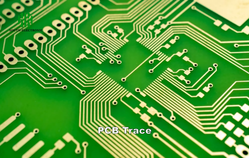
Proper impedance control ensures smooth signal flow by matching transmission line resistance (typically 50Ω for WiFi) to component specifications, preventing reflections that distort data packets and reduce network throughput.
Tuning Your Signal Highway
| Factor | Impact on Impedance | Mitigation Strategy |
|---|---|---|
| Trace Width | Wider traces = lower Z | Use impedance calculators |
| Dielectric Height | Thinner dielectrics = higher Z | Prefer consistent laminate thickness |
| Copper Weight | Thicker copper lowers Z | Match plating to design specs |
| Solder Mask | Adds capacitive loading | Apply selectively on critical traces |
For 5GHz WiFi signals, even a 10% impedance mismatch can cause 30% signal loss. That’s why modern PCB stackups[^5] use tightly controlled dielectric materials like Isola 370HR, with ±5% impedance tolerance. Differential pairs for high-speed data lines require precise spacing – a 5 mil gap variation can ruin signal integrity.
What Are the Key EMI Challenges in WiFi PCB Layout?
Your smart speaker mysteriously disconnects whenever the microwave runs? That’s EMI chaos unleashed by poor PCB layout practices fighting over crowded airwaves.
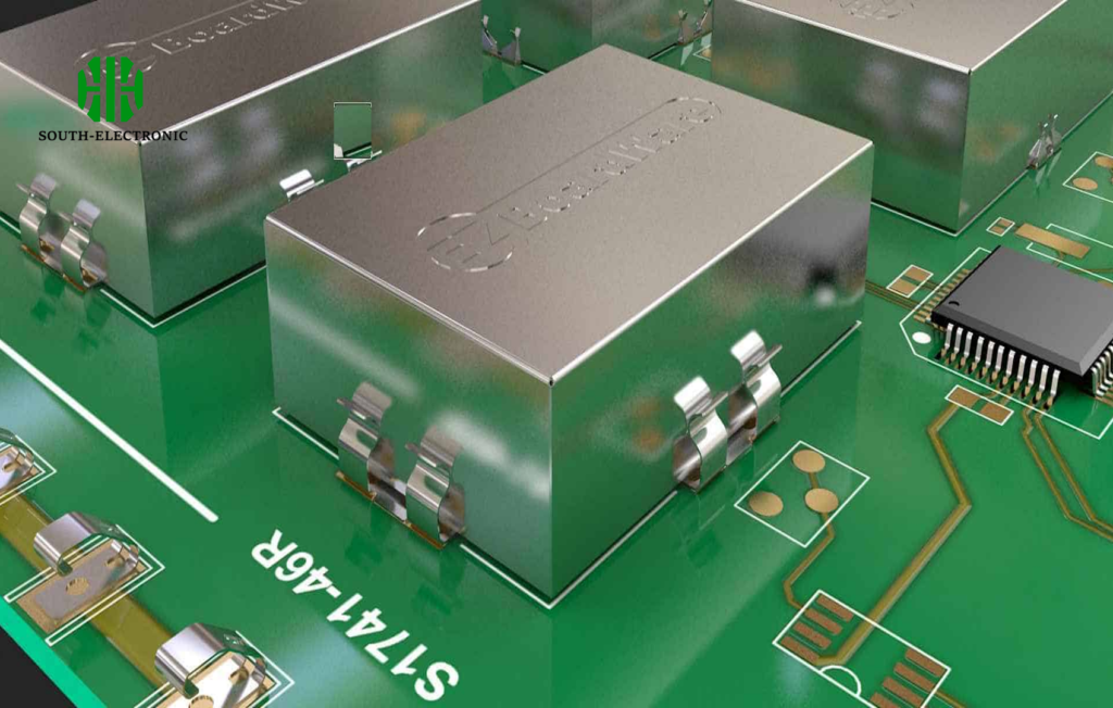
Primary EMI challenges include unintended antenna effects from long traces, common-mode noise from unbalanced circuits, and crosstalk between digital/RF sections – all of which degrade WiFi signal clarity and reliability.
Taming the RF Storm
| EMI Source | Impact | Countermeasure |
|---|---|---|
| Ground Loops | Creates noise antenna | Star grounding topology |
| Via Stubs | Reflect high-frequency signals | Use back-drilled vias |
| Component Radiation | Localized interference | Shield cans over noise sources |
| Power Noise | Modulates RF signals | Multiple decoupling capacitors |
Ground plane design proves crucial here. A split plane approach isolates noisy digital grounds from sensitive RF circuits, connected at a single point to prevent ground loops. For 802.11ax routers operating in dense environments, harmonic suppression techniques like π-filters on power lines become essential.
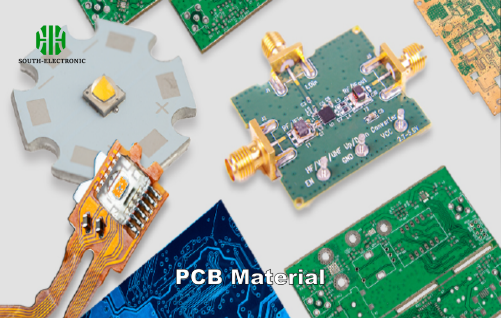
Which PCB Material Types Are Best for High-Speed WiFi Designs?
Using standard FR4 for a WiFi 6E board is like racing a minivan in Formula 1 – thermal runaway and signal loss guaranteed without proper material selection.
Optimal materials balance low dielectric loss[^6] (Df < 0.004) with stable permittivity across frequencies. Rogers 4350B[^7] dominates high-end applications with 0.0037 Df at 10GHz, while Isola's TerraGreen offers eco-friendly performance for budget-conscious designs.
Material Showdown
| Material | Dk (10GHz) | Df (10GHz) | Thermal Performance | Cost |
|---|---|---|---|---|
| Standard FR4 | 4.5 | 0.020 | Poor | $ |
| Rogers 4350B | 3.48 | 0.0037 | Excellent | $$$$ |
| Isola I-TERA MT40 | 3.45 | 0.007 | Good | $$ |
| Taconic TLY-5 | 2.2 | 0.0009 | Fair | $$$$ |
For 6GHz WiFi 6E designs, material choice becomes critical. While Rogers substrates offer best-in-class performance, their $500/sheet cost pushes many designers toward hybrid stackups. Strategic use of high-speed materials only in RF stages keeps budgets manageable without sacrificing signal integrity.
Conclusion
Successful WiFi PCB design hinges on four pillars: core component selection, impedance control, EMI mitigation, and material optimization. Master these elements to create reliable, high-performance wireless devices that users never think about – until they try inferior products.
[^1]: Explore this link to understand the intricacies of WiFi PCBs and their role in modern connectivity.
[^2]: Learn about radio frequency transceivers and their critical role in wireless communication systems.
[^3]: Discover the significance of impedance-matched antennas in enhancing WiFi signal quality and range.
[^4]: Understanding impedance mismatches is crucial for optimizing WiFi performance and avoiding signal loss. Explore this link for in-depth insights.
[^5]: Discover how the design of PCB stackups can significantly impact WiFi signal integrity and performance, ensuring better connectivity.
[^6]: Understanding dielectric loss is crucial for optimizing PCB materials, enhancing signal integrity and overall device performance.
[^7]: Explore the advantages of Rogers 4350B for high-speed applications, ensuring optimal performance and reliability in your designs.

