What is advanced PCB?
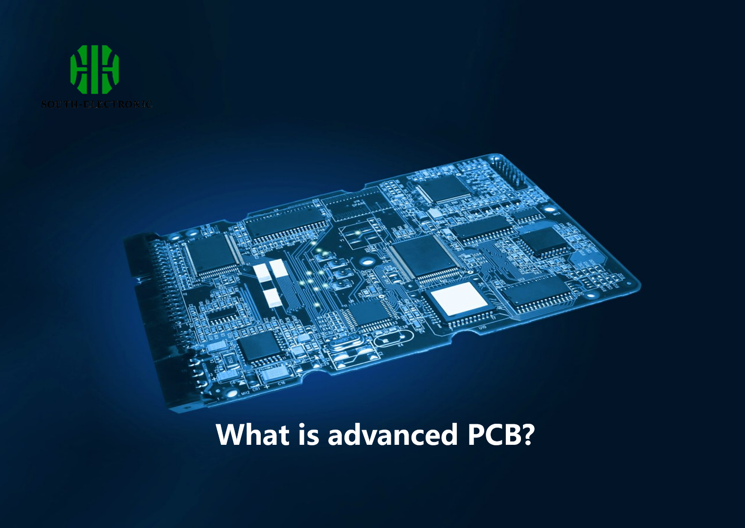
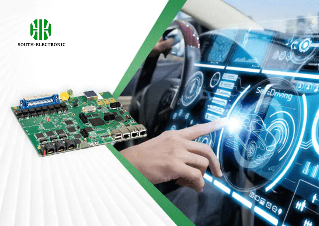
Advanced PCBs, or Printed Circuit Boards, are specialized circuit boards designed with enhanced features and capabilities. They support complex electronic functions, high-speed applications, and improved reliability, making them essential in cutting-edge technology sectors like telecommunications, medical devices, and aerospace.
Types of Advanced PCBs
- High-Density Interconnect (HDI) PCBs: These feature fine lines and spaces, smaller vias, and higher connection pad density than traditional PCBs.
- Flexible PCBs: Made with flexible materials, allowing them to bend during use, which is ideal for compact and dynamic applications.
- Rigid-Flex PCBs: Combine the technologies of rigid and flexible PCBs, offering a hybrid solution that can be bent or folded while maintaining the functionality of rigid areas.
- Multilayer PCBs: Consist of three or more double-sided boards stacked together, with very high connection density.
Features and Characteristics of Advanced PCB
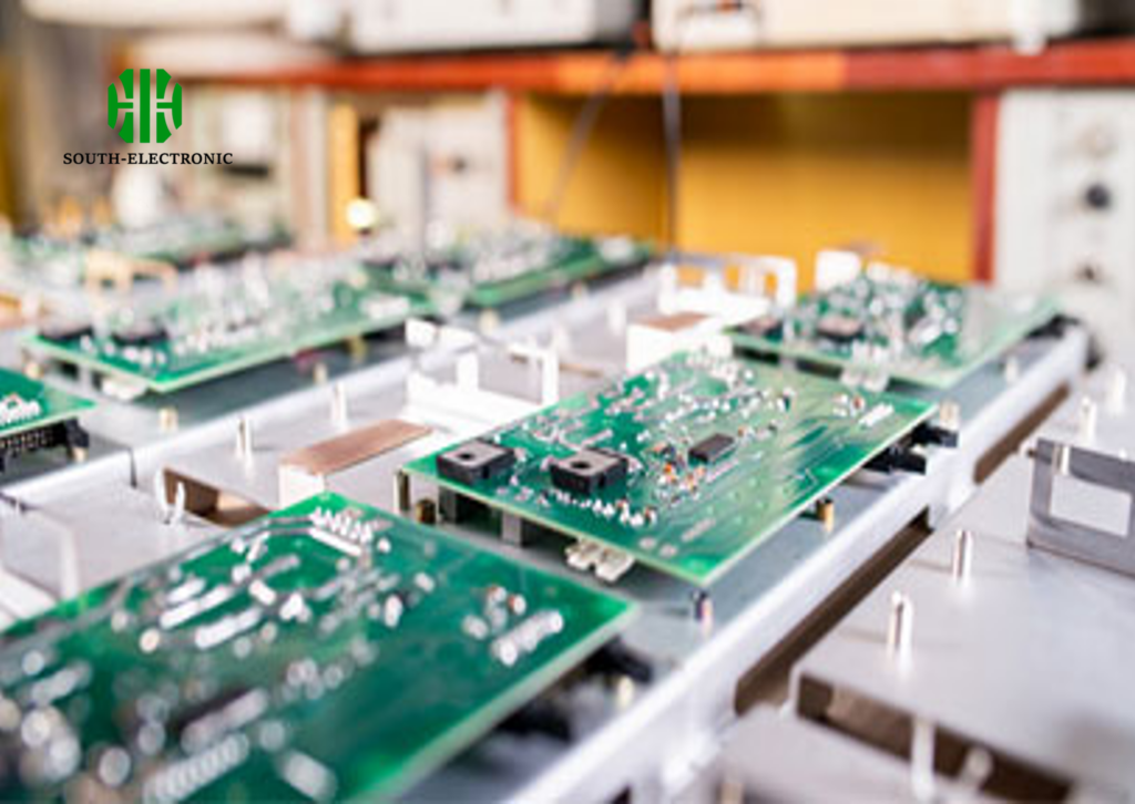
- High Performance and Reliability: Designed to withstand extreme conditions including high temperatures, pressures, and frequencies.
- Increased Density: Support more components per unit area through techniques like via-in-pad and microvias.
- Enhanced Signal Integrity: Reduction in signal loss and cross-talk, beneficial in high-speed applications.
- Thermal Management: Advanced PCBs often incorporate materials and designs that help manage heat generation more effectively.
Difference Between Standard and Advanced PCB
The key differences between standard and advanced PCBs lie in their complexity, materials used, and performance capabilities.
| Feature | Standard PCB | Advanced PCB |
|---|---|---|
| Layers | 1-2 | Multiple |
| Material | Standard FR-4 | High-performance materials |
| Density | Low | High |
| Performance | Moderate | Enhanced |
| Applications | Consumer electronics, basic devices | Telecommunications, aerospace, medical devices |
Advanced PCB Manufacturing Techniques
- Laser Drilling: Used for creating microvias with high precision.
- Direct Imaging Techniques: Enhances the precision of the patterning process.
- Automated Optical Inspection (AOI): Ensures high quality by detecting faults early in the manufacturing process.
- Sequential Lamination: Allows for the creation of multilayer PCBs with different material properties or varying layers of circuitry.
Advanced PCB Assembly Processes
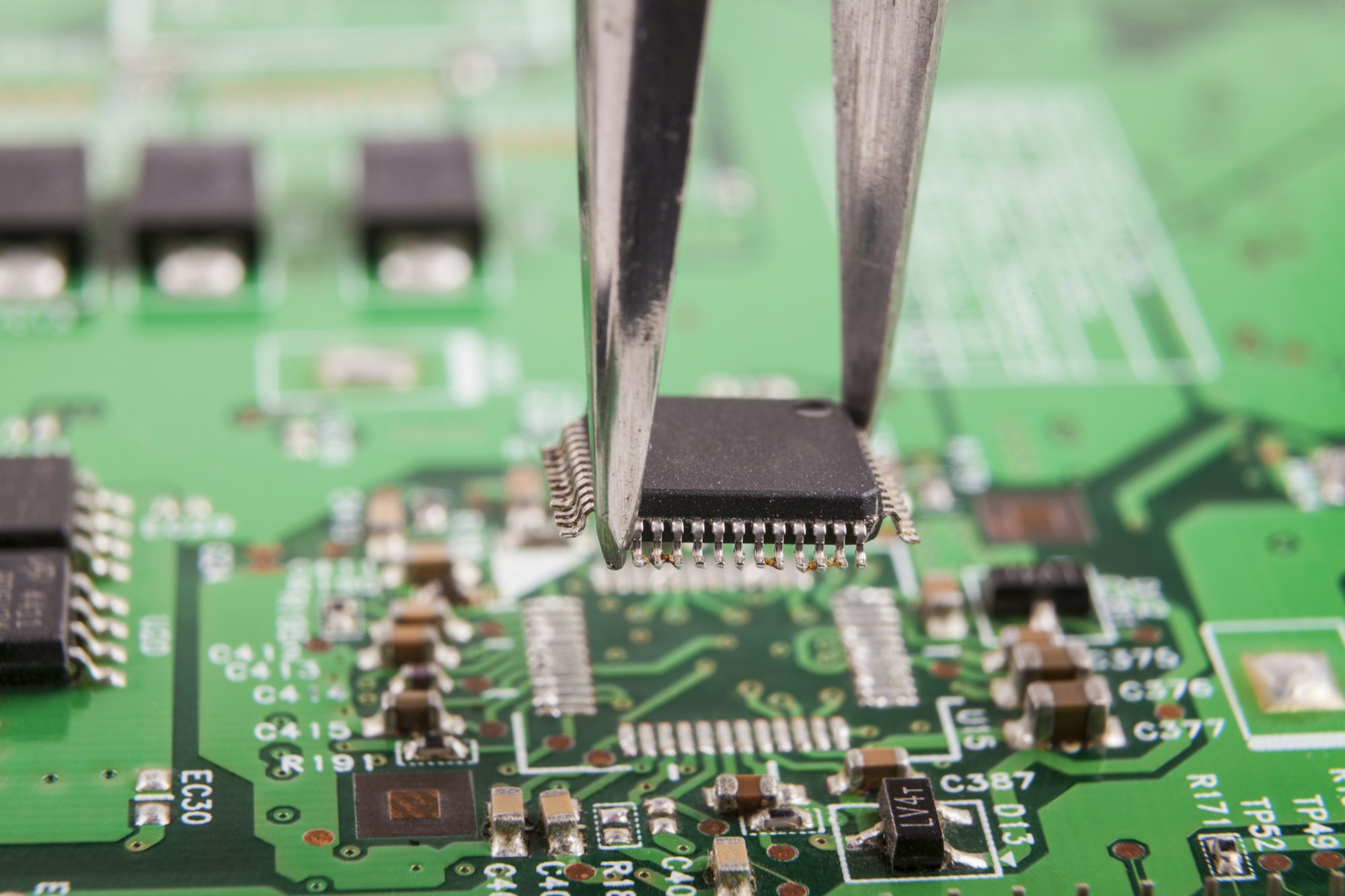
- Surface Mount Technology (SMT): Components are mounted directly onto the surface of the PCB, allowing for more components on a smaller area.
- Pin-in-Paste (PiP) Technique: Combines through-hole and SMT techniques by inserting pins through paste-covered holes.
- Selective Soldering: Precisely solders components without damaging nearby heat-sensitive parts.
- 3D Assembly: For more compact and vertically integrated electronic devices, where components are placed in a three-dimensional space.
Advanced PCBs are at the heart of modern electronic applications that require high precision and reliability. These boards are characterized by their high circuit density and the ability to support sophisticated features, making them indispensable in cutting-edge technological solutions.
If you have any questions or need further information about PCB technologies, feel free to leave a comment below. Don’t forget to share this article if you found it useful, and stay connected for more insights into the fascinating world of electronics!

