
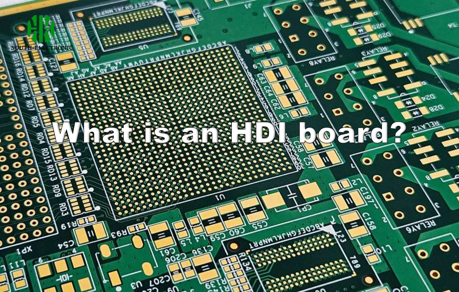
You ever wonder why your phone keeps getting thinner but smarter? Traditional PCBs hit physical limits. HDI boards break those barriers.
HDI stands for High Density Interconnect. These circuit boards pack more wiring in less space using micro-blind and buried vias. They create pathways 20% narrower than standard PCBs, enabling smaller, more powerful electronics.
Now that we’ve defined HDI, let’s clear up common misunderstandings around this technology. Key differences exist that many overlook.
Are all PCBs with blind and buried vias HDI?
Seeing "blind vias" on specs doesn’t automatically mean HDI. Many engineers assume otherwise. This misconception impacts design choices.
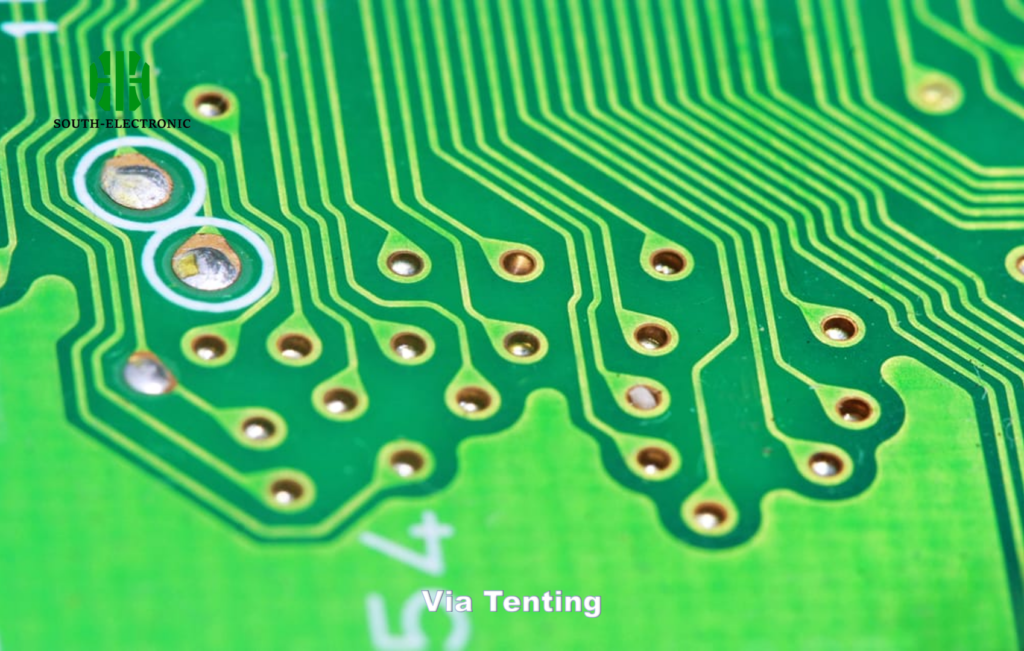
Not every PCB with blind/buried vias qualifies as HDI. True HDI requires additional density features: micro-vias under 150μm diameter AND conductor spacing below 100μm. Vias alone don’t define the technology.
Three Critical HDI Defining Features
We break down the density requirements distinguishing HDI from other boards with similar features:
| Feature | Standard PCB | HDI Board |
|---|---|---|
| Via Diameter | >200μm | ≤150μm |
| Line Width/Spacing | >100μm | ≤100μm |
| Layer Buildup | Single step | Sequential lamination |
| Via Technology | Through-hole only | Micro-blind/buried + filled |
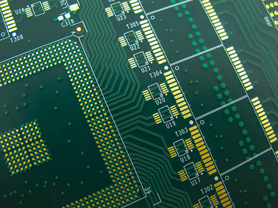
Simple vias don’t deliver high density alone. Micro-vias and tight spacing shrink pathways 60%. Sequential lamination stacks conductive layers like compressed pancakes. This combination handles twice as many components versus a same-sized normal board.
How do you differentiate between first-order, second-order, and third-order HDI boards?
Manufacturers tout "high-order HDI" as superior. Yet few explain what those levels actually change functionally. Let’s demystify the order system.
Orders indicate build-up complexity: First-order has one micro-via layer. Second-order connects two layers with staggered vias. Third-order adds stacked micro-vias and requires laser drilling.
Building Complexity From Ground Up
Think of orders as adding floors to a building – each increases structural demands:
First-Order HDI Characteristics
Like basic scaffolding. Single micro-via layer connects adjacent layers. Handles moderate complexity: 6-8 layers. Used in smartwatches. Production time: 3-5 days.
Second-Order HDI Differences
Adds diagonal connections. Staggered vias allow skipping layers. Enables >10 layers. Requires partial stacking. Common in medical sensors. Adds 40% manufacturing steps.
Third-Order HDI Capabilities
Full stacked micro-vias bridge non-adjacent layers. Laser-drilled holes under 75μm. Features filled copper plating in holes. Found in satellite components. Costs 3x first-order.
What are the differences between HDI boards and regular PCBs?
Regular PCBs still dominate simple electronics. But they collapse when pushed too hard. See why HDI replaces them in premium applications.
Key differences show why HDI outperforms: 8x wiring density, 3x thermal dissipation, and 50% better signal integrity. Plus HDI supports 0.3mm pitch BGAs – impossible for standard PCBs.

Side-By-Side Performance Breakdown
Standard PCBs cap out where HDI begins to shine. Compare critical specs:
| Parameter | Standard FR-4 PCB | HDI Board | Advantage |
|---|---|---|---|
| Min. trace width | 127μm | 50μm | 61% thinner |
| Vias per cm² | 20 | 130 | 550% more |
| Layer transitions | Through-vias only | Any-layer micro-vias | Flexible routing |
| Max. layer count | 20 | 60+ | Scalability |
| Signal loss | High over 3GHz | Low up to 10GHz | Speed capacity |
HDI’s any-layer connections reduce signal path lengths 40%. This cuts interference. Thin traces fit 5x more transistors. HDI handles 100W/mm² thermal load versus 30W on standard boards. For wearables and aeropace, these numbers make or break designs.
Conclusion
HDI boards enable today’s miniaturized tech with their micro-via architecture and layered builds. They outperform regular PCBs where density matters most. Essential for cutting-edge devices.

