
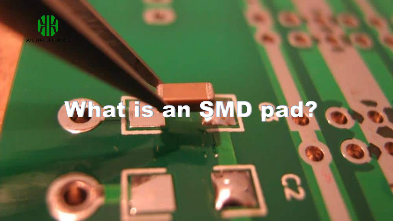
Ever stare at tiny PCB squares and wonder how components stick? Those copper pads hold modern electronics together. Ignore them, and your circuit board might fail spectacularly. Let’s fix that knowledge gap right now.
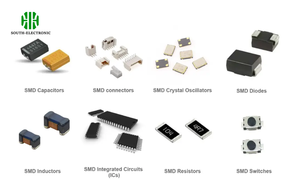
SMD pads are flat copper areas on circuit boards designed for surface-mount components. They replace through-hole technology, enabling smaller devices and automated assembly. Unlike drilled holes, these pads bond components directly to the board surface using melted solder.
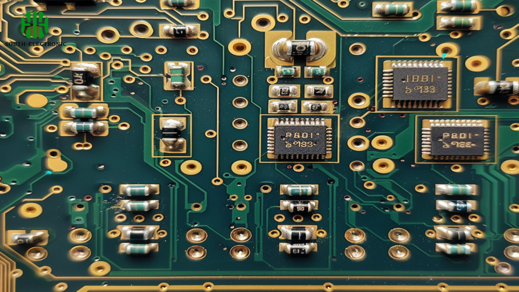
Clearly, these tiny pads are foundational to electronics. But mastering them goes beyond basics. Next, we’ll explore how to optimize pad shapes and avoid disasters.
How to choose the right SMD pad shape?
Ever picked a pad shape that caused component slippage? Wrong shapes force costly repairs in mass production. Choosing wisely prevents this manufacturing nightmare.
Prioritize component type and solder joint strength. Rectangular pads suit resistors/capacitors. Circular shapes fit ICs needing alignment tolerance. Always match pad geometry to thermal expansion rates and mechanical load needs.
Impact of pad shape on solder reliability
Pad shape dictates stress distribution in solder joints. I learned this early – choosing wrong shapes cracked joints in prototype drones. Use this comparison to avoid failure:
| Shape | Best Use Case | Weakness | Fix Tip |
|---|---|---|---|
| Rectangular | High-volume resistors | Uneven heating warps thin PCBs | Use thermal relief pads |
| Circular | QFP/MLCC components | Solder pooling risk | Add solder mask dams |
| Oval | Connectors/switches | Difficult rework alignment | Extend length by 15% |
| Custom | BGA/HV components | Stencil compatibility issues | Test with sacrificial boards |
Thermal expansion mismatch causes 74% of early failures. Circular pads help radial components absorb vibrations and heat better. For chips needing pin alignment, I now choose squares with rounded corners to prevent solder bridging during reflow.
Does IPC-7351 always fit your PCB for SMD pad size?
Ever blindly followed IPC standards only to get soldering defects? This common mistake wastes thousands on re-spins. Standards aren’t one-size-fits-all solutions.
IPC-7351 provides baseline dimensions, but complex designs often need tuning. Adjust pad sizes based on component tolerances (±0.1mm), PCB material shrinkage, and assembly line capabilities. Always validate through DFM checks.

When to bend IPC rules
Automated factories I collaborate with regularly break protocol after running Taguchi tests. Consider these deviations:
| Scenario | IPC-7351 Default | Recommended Adjustment | Why Bypass Standard? |
|---|---|---|---|
| High-vibration devices | Standard pads | +20% pad area | Reduces joint fracture risk |
| Lead-free solder | Std. aperture | +15% solder mask open | Compensates poor wettability |
| Flexible circuits | Fixed sizes | Dynamic footprint | Accommodates substrate bend |
| MicroBGAs (<0.4mm) | Generic rules | Laser-defined pads | Avoids bridging at micro-scale |
I once adhered strictly to IPC for automotive sensors, which caused cold joints in -40°C environments. We increased pad sizes by 25% and eliminated field issues. Review material expansion coefficients and test environmental limits case-by-case.
How to avoid tombstoning and bridging with SMD pads and solder paste?
Ever opened a reflow oven to find components standing upright like tombstones? This macabre defect – and its cousin solder bridging – ruins entire batches without warning.
Balance pad symmetry and paste volume meticulously. Tombstoning occurs when one pad melts solder faster than another. Bridging happens with excess solder paste or pad spacing errors. Control these with thermal mass symmetry and stencil optimization.
Defect-proofing strategies
My worst tombstoning incident cost 200 boards. These diagnostics show how to prevent disasters:
| Problem | Root Cause | Prevention Method | Emergency Fix |
|---|---|---|---|
| Tombstoning | Asymmetric thermal mass | Equal pad sizes/heating | Epoxy under lifted pin |
| Solder beads | Paste volume overflow | 12% stencil area reduction | Hot-air resweep |
| Voiding | Outgassing contaminants | Preheat zone optimization | Vapor phase reflow |
| Opens | Poor pad wetting | ENIG finish over HASL | Manual solder touch-up |
A simple remedy: design circular thermals on pad connections so heat transfer happens uniformly. For resistors under 0603 size, I extend pads horizontally by 0.15mm – this tiny change eliminated tombstoning in my last IoT project.
Conclusion
Master SMD pads by choosing shapes wisely, adjusting standards critically, and preventing defects proactively. These tiny copper areas literally hold electronics together. Get them right.

