
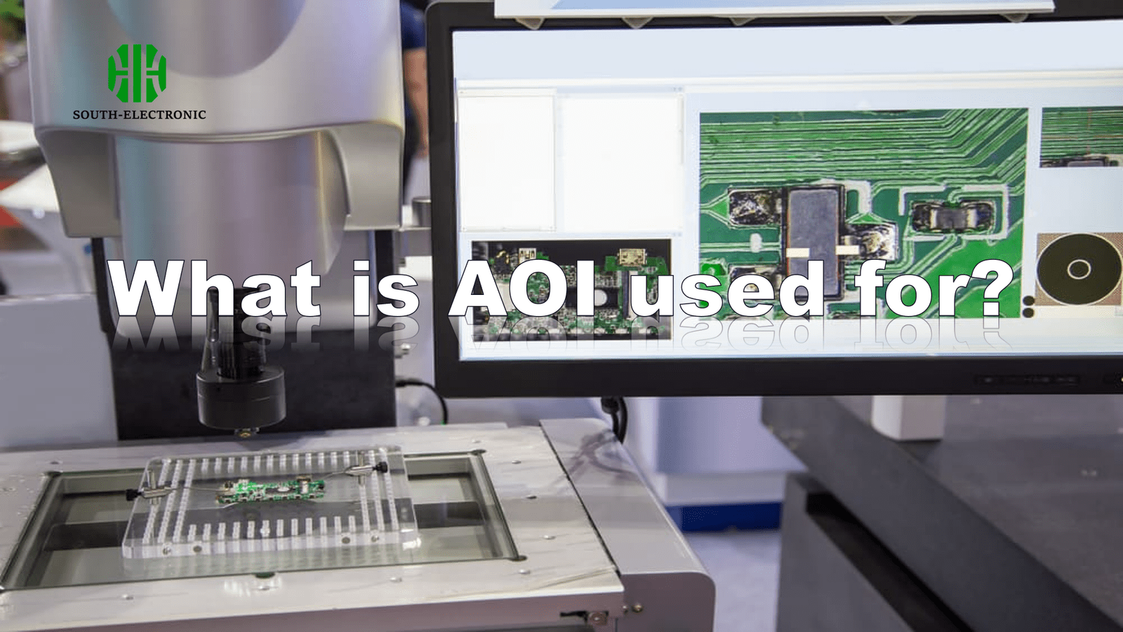
Manufacturers lose millions yearly to unseen defects escaping production. Damaged reputations and customer returns hurt profits deeply. Automated Optical Inspection (AOI) solves this invisible threat effectively.
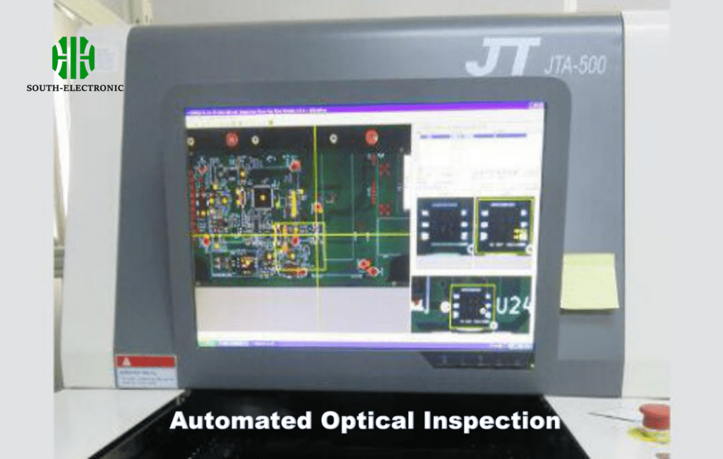
AOI uses high-resolution cameras to scan printed circuit boards for flaws immediately after assembly. It detects solder defects, missing components, and placement errors reliably, ensuring manufacturing standards remain high. This process replaces unreliable manual checks and reduces defect escape.
Now you know AOI’s core purpose. But modern manufacturing involves other inspection methods too. Understanding AOI fully means seeing its place among techniques like ICT and X-ray. Let’s examine these concepts step by step.
What is automated vision inspection (ICT)?
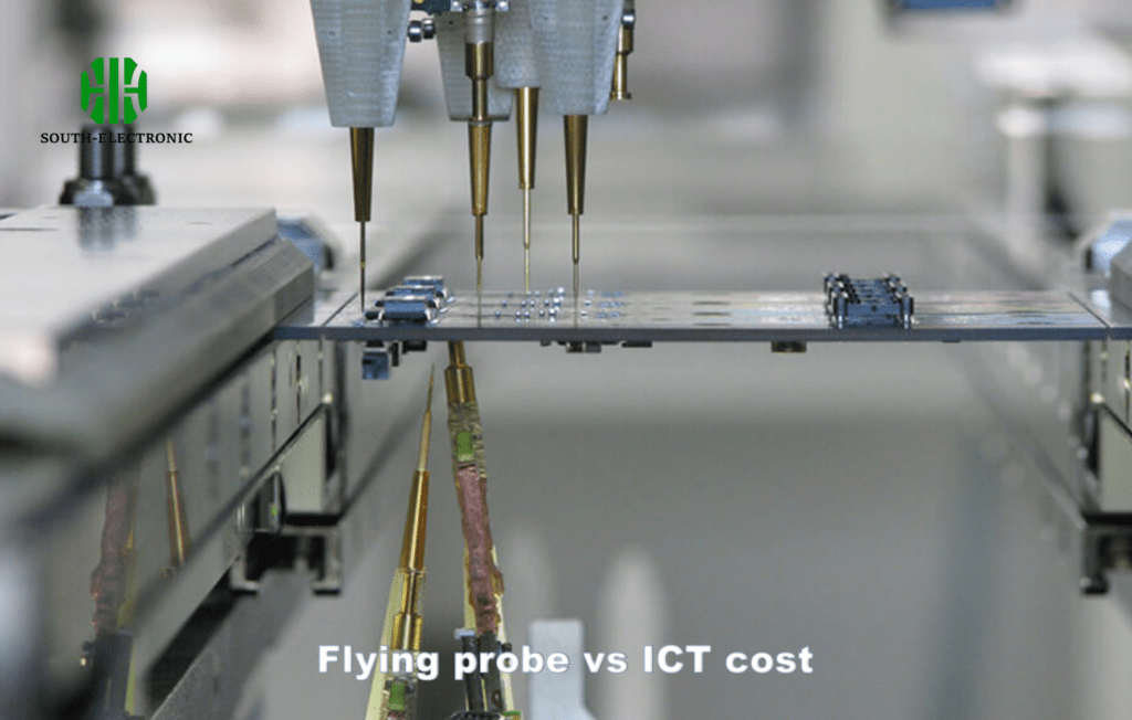
Circuit board failures halt production lines and delay critical orders. Finding faults takes hours without smart systems. In-Circuit Test (ICT) eliminates this pain differently than AOI.
ICT uses electrical probes to check component functionality on assembled PCBs. Unlike AOI, it directly measures resistance and capacitance values. This confirms parts work correctly beyond visual appearance.
Visual vs electrical inspection
AOI and ICT serve distinct purposes in quality control:
| Aspect | AOI | ICT |
|---|---|---|
| Method | Camera-based optical scans | Physical electrical probes |
| Detection Focus | Surface defects like solder issues | Electrical faults like open circuits |
| Stage Used | Early assembly phase | Functional testing phase |
| Speed | Very fast (seconds per unit) | Slower due to physical probing |
| Component Depth | Shallow (surface examination) | Deep (tests component functions) |
ICT validates whether components work at electrical levels beyond AOI cameras. For example, an AOI might spot misplaced resistors visually. But only ICT can reveal if those resistors electrically function after soldering. Both systems form complementary stages in verification. Manufacturers often run AOI first to catch obvious errors before investing time in ICT.
What is the difference between AOI and ICT?
Mistaking AOI for ICT causes misconfigured quality control lines. Repair costs skyrocket when flaws bypass both systems. Confusing their roles invites expensive recalls.
AOI is optical and identifies physical defects through images. ICT is functional and tests electrical performance physically. They inspect different quality dimensions so factories need both for comprehensive results.
How they complement each other
Let’s explore why AOI and ICT coexist rather than compete:
-
Defect detection layers
AOI catches visible surface issues before boards advance. ICT tests underlying performance next. This dual-layer approach prevents electrical rework caused by overlooked physical flaws. -
Timing optimization
AOI scans boards faster—ideal for early production monitoring. ICT takes longer but verifies operational integrity near assembly end. Combining both improves efficiency while reducing bottlenecks. -
Cost balancing
Manufacturers get wider defect coverage without doubling equipment expenses. AOI stops minor problems early. ICT catches complex electrical failures. Using a single system leaves dangerous blind spots in quality control.
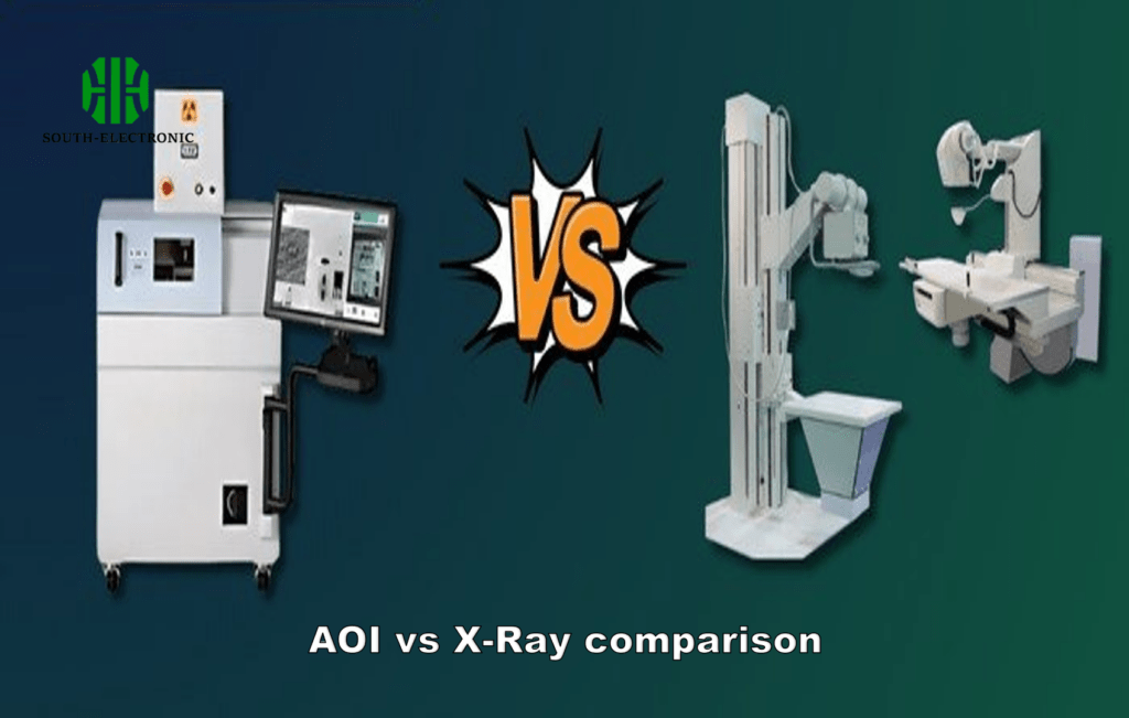
Can AOI completely replace X-ray inspection in PCB assembly?
Hidden solder joints under chips ruin entire PCB batches. But X-ray machines are expensive investments. Can manufacturers just rely on AOI? Definitely not.
No, AOI cannot replace X-ray for inspecting hidden solder connections. While AOI examines surface components easily, X-ray penetrates materials revealing internal flaws like voiding and sub-surface cracks reliably.
Why both processes remain essential
Let’s analyse inspection roles for complex PCB structures:
| Factor | AOI | X-ray |
|---|---|---|
| Surface components | Excellent | Limited |
| Ball Grid Arrays | Blind spots | Full view |
| Internal layers | Can’t inspect | Detailed |
| Solder joints | Exposed only | Even buried |
X-ray excels inside boards AOI optics can’t physically access. Areas needing buried connections require X-ray validation. Lead-free solder joints also form internally and demand depth checking.
AOI remains essential for surface-mounted parts and visible defects. But bypassing X-ray leads to undiagnosed failure risks especially in multilayer boards. Smart factories use AOI for quick scans and X-ray for deep verification.
Conclusion
AOI provides fast visual defect detection vital for surface components while ICT tests circuit performance. Neither substitutes X-ray which inspects hidden solder joints essential for complex assembly quality and reliability. Use all three.


