

Are your circuit boards failing? Tiny components ruin reliability? BGA soldering solves modern electronics’ toughest connection problems.
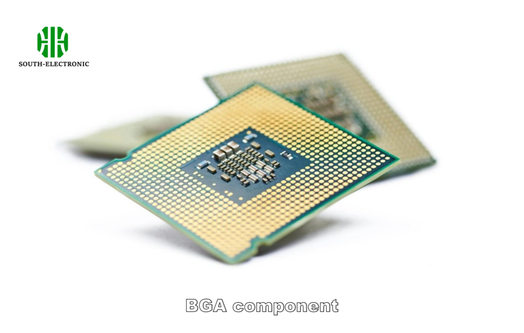
BGA soldering attaches chips using microscopic solder balls. It replaces fragile legs with a grid of melted spheres. This technique lets tiny chips handle high power and speeds. Proper BGA methods prevent connection failures in phones and computers.
Traditional soldering struggles with today’s electronics. BGA techniques are different. Let’s explore common challenges and solutions.
How to avoid common BGA soldering defects like bridging and voids?
Defective BGA joints cause mysterious crashes? Hidden flaws destroy devices later? Control your process to prevent expensive rework.
Stop defects through precise solder volume control. Clean surfaces guarantee strong bonds. Correct oven temperatures prevent bubbles and shorts. Visual guides catch errors early.

Breaking down defect prevention strategies
Two main problems plague BGA joints:
Bridging causes short circuits
Adjacent solder balls melt together. This happens with too much solder paste or uneven heating. Use exact stencil thickness. Limit paste application to ball contact points. Slow heating gives paste time to flow correctly.
Voids create weak connections
Air pockets hide inside solder balls. They crack under heat stress. Moisture causes most bubbles. Bake components to remove dampness before assembly. Temperature curves matter greatly:
| Stage | Purpose | Void Reduction Tip |
|---|---|---|
| Preheat | Gentle warm-up | Ramp below 2°C/second |
| Soak | Activate flux | Hold 60-90 seconds |
| Reflow | Melt solder | Peak 230-250°C |
| Cooling | Solidify joints | Fast cooling rate |
Flux type affects bubble formation. Low-volatility fluxes trap fewer air pockets. Check oven temperature with multiple sensors. Test with artificial defects first. Small changes prevent big failures later.
What equipment is essential for successful BGA soldering?
Inconsistent results frustrate you? Wasted parts drive costs up? The right tools guarantee first-time perfection.
Critical tools ensure precise connections. Stencils apply exact solder amounts. Reflow ovens control temperature perfectly. X-rays see hidden flaws inside joints. Microscopes spot surface issues others miss.

Must-have tools explained
Three categories cover your needs:
Preparation equipment
Laser-cut stainless steel stencils manage paste volume. I match aperture sizes to ball diameters. Cleaning stations remove oxidation. Baking ovens dry components for 8 hours at 125°C before assembly.
Soldering systems
Forced convection reflow ovens work best. They must have 10+ heating zones and nitrogen injection. BGA rework stations combine heating elements and vacuum pickups. Preheating plates stop heat damage to surrounding parts. Thermocouples monitor actual board temperatures.
Inspection gear
Digital microscopes examine placement at 50x zoom before heating. X-ray machines reveal problems inside joints. My minimum requirement: 130kV systems with digital imaging. Thermal cameras confirm even heat distribution across boards.
Dedicated software analyzes X-ray images automatically. This catches voids below 25% diameter before they break. Remember: Good tools cost less than scrapped boards.
How to inspect BGA solder joints for quality?
Failed boards pass visual checks? Customers return "working" devices? Effective inspection finds hidden defects early.
Use X-rays to see inside joints. Track shape problems and bubble sizes. Measure connections against industry standards. Compare results across production runs.

Evaluation methods that work
Inspection happens at three stages:
Pre-reflow checks
Measure solder paste deposits after printing. Target 75-85% coverage of pad area. Check component alignment with optical systems. Even 0.1mm shifts cause joint failures. Record positions before heating for later comparison.
Post-reflow evaluation
Use automated X-ray systems to examine joints. Look for:
- Ball spacing (bridging shows touching circles)
- Void distribution (over 15% = replace joint)
- Ball collapse (height indicates connection strength)
Good joints show round shapes and consistent spacing. Bad joints appear squashed or mismatched.
Destructive testing samples
Cut random boards weekly to test. Shear tests measure connection strength. Cross-sections reveal internal structures. Peel tests check pad adhesion. I find microscopic cracks this way before field failures happen.
Modern software color-codes problems in scans. Red zones show immediate defects. Yellow flags need monitoring over time. Continuous measurement prevents customer complaints.
Conclusion
BGA soldering solves modern electronics challenges. Correct equipment prevents defects. Precise inspection ensures durability. Master these steps for reliable circuit boards.

