
Ever wondered how electricity flows seamlessly through your smartphone? Copper foil PCB makes it possible. These thin copper layers form the conductive pathways powering every circuit. But what happens when this critical component fails? Let’s uncover its role.
Copper foil PCB[^1] uses a thin layer of copper laminated onto insulating material to create electrical connections. It determines current capacity[^2], thermal management[^3], and signal integrity. Common thicknesses range from 0.5 oz/sq ft (17 µm) to 2 oz/sq ft (70 µm).
Understanding copper foil is essential for anyone designing or repairing circuit boards. Below, we’ll explore types, thickness trade-offs, manufacturing flaws, and quality tests to optimize your PCB projects.
What Is Copper Foil PCB and How Does It Work in Electronic Circuits?
Copper foil forms conductive paths etched from a copper-clad laminate. These traces connect components while the insulating base prevents short circuits. The foil thickness controls current capacity and heat dissipation.
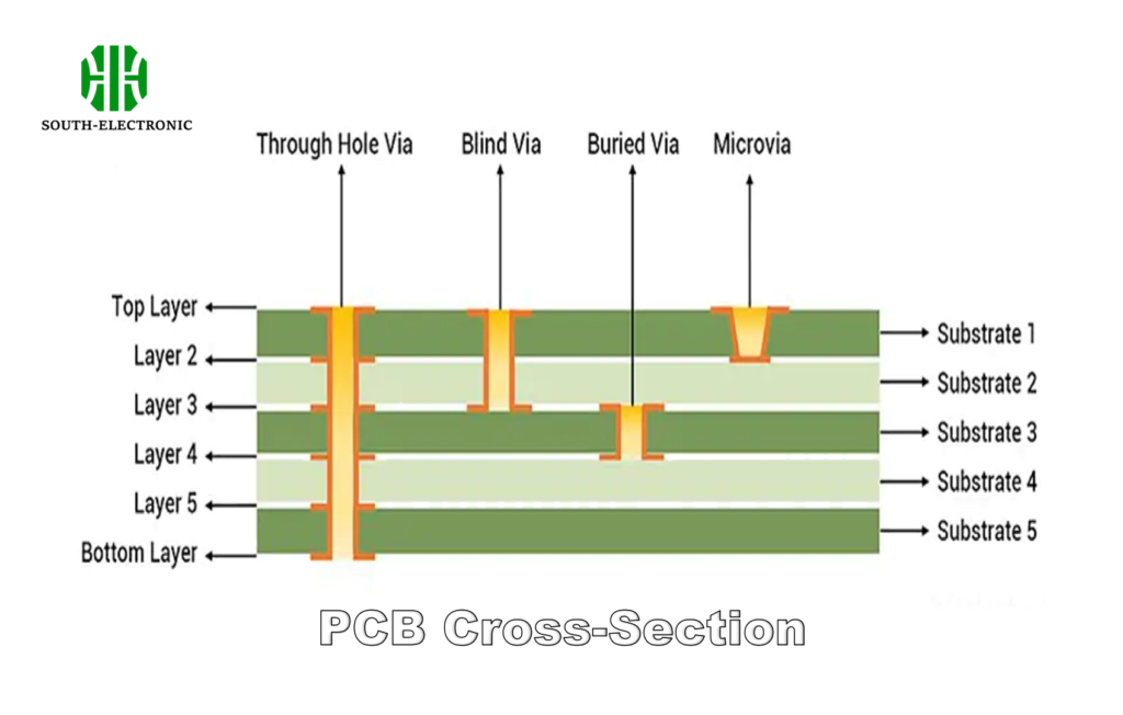)
How Copper Foil Enables Circuit Functionality
Copper foil serves three primary functions:
-
Electrical Pathways
- Carries signals between ICs, resistors, and capacitors
- Thicker foils handle higher currents without overheating
-
Thermal Management
- Spreads heat from components like processors
- 2 oz copper vs 1 oz comparison:
| Thickness (oz/sq ft) | Max Current (10°C rise) | Thermal Resistance |
|---|---|---|
| 1 | 3.5A | 0.5°C/W |
| 2 | 6.8A | 0.2°C/W |
- Mechanical Support
- Reinforces PCB structure
- Prevents warping during soldering
Designers choose thickness based on current demands and space constraints. Thin foils (0.5 oz) work for low-power devices, while power supplies need 2-4 oz copper.
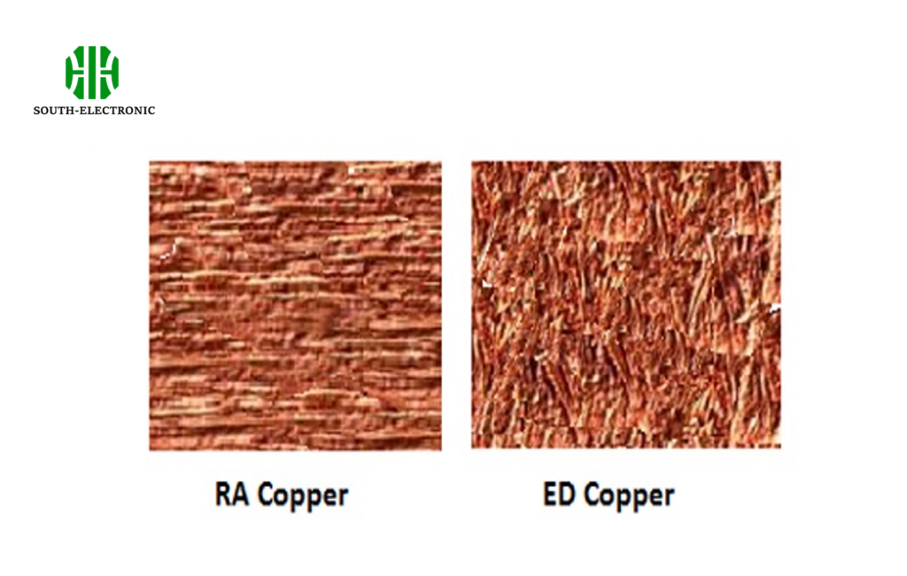
What Are the Key Differences Between Rolled and Electrodeposited Copper Foil?
Think of copper fabrication methods like forging vs casting. The production technique drastically changes material properties.
Rolled copper[^4] undergoes mechanical compression, creating uniform grain structures. Electrodeposited (ED) copper[^5] uses electrolysis, resulting in vertical crystal growth. Rolled foils excel in flexibility; ED copper dominates cost-sensitive applications.
)
Choosing Between Rolled and Electrodeposited Copper
Four critical factors differentiate these copper types:
1. Grain Structure
- Rolled: Layered grains → Better bend tolerance
- ED: Columnar grains → Prone to cracking when flexed
2. Surface Roughness
- Rolled: Smoother surface (Ra 1.0-2.0 µm)
- ED: Rougher texture (Ra 3.0-5.0 µm) → Better adhesion
| 3. Cost Comparison | Type | Relative Cost | Production Speed |
|---|---|---|---|
| Rolled | 2x | Slow | |
| Electrodeposited | 1x | Fast |
4. Application Matches
- Rolled: Flexible circuits, aerospace
- ED: Rigid boards, consumer electronics
Most PCBs use ED copper due to lower costs, but high-reliability systems need rolled copper’s durability.
How Does Copper Foil Thickness Impact PCB Performance and Cost?
Picture water pipes – narrow ones limit flow, while wider ones cost more. Copper thickness[^6] follows similar logic.
Thicker foils handle higher currents but increase material costs. 1 oz copper (35 µm) balances cost/performance for most uses. Doubling thickness (2 oz) quadruples copper weight, raising PCB costs by 30-50%.
)
Balancing Thickness Trade-Offs
Three critical considerations when selecting copper weight:
1. Current Requirements
- Formula: Required thickness (oz) = (Current in Amps)/3.5
2. Thermal Effects
- Thin copper overheats → solder joint failures
- Thermal simulation example:
| Thickness | Temperature Rise @ 5A |
|---|---|
| 0.5 oz | 68°C |
| 1 oz | 32°C |
| 2 oz | 14°C |
3. Manufacturing Limits
- Fine traces need thin copper:
- 0.5 oz: 3 mil lines
- 2 oz: 8 mil minimum
Use thinner copper for signal lines, thicker for power planes. Always verify with your PCB fabricator’s capabilities.
Manufacturing and How to Fix Them?
Even Superman has kryptonite. Copper foil issues can cripple boards if not addressed.
Common defects include pitting, over-etching, and adhesion failure. 70% of copper-related failures trace back to contamination during manufacturing. Proper cleaning and process control prevent most issues.
)
Troubleshooting Copper Foil Problems
Solve these frequent manufacturing challenges:
1. Delamination During Soldering
- Cause: Moisture absorption
- Fix: Bake PCBs at 120°C for 4 hours pre-assembly
2. Uneven Etching
- Cause: Incorrect etchant temperature
- Solution: Maintain FeCl3 at 45-50°C
3. Copper Pitting[^7]
- Root Cause: Contaminated laminate
- Prevention: ISO Class 6 cleanroom handling
4. Skin Effect in High-Frequency Boards
- Mitigation: Use rolled copper with smooth surface
Regular AOI (Automated Optical Inspection) catches 95% of copper defects before assembly.
How to Test and Ensure Quality of Copper Foil in PCB Production?
Would you trust a bridge without stress tests? PCB copper requires rigorous quality checks.
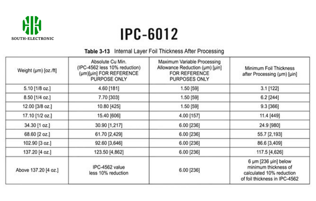
Key tests measure thickness, peel strength, and conductivity. X-ray fluorescence (XRF) verifies copper weight within ±10%. Peel tests require 1.4 N/mm strength for reliable adhesion.
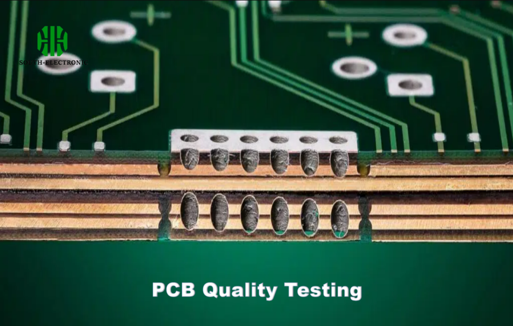)
Implementing Copper Foil QC
Four essential quality control steps:
-
- Method: Cross-section microscopy
- Tolerance: ±10% of nominal value
-
Adhesion Testing
- Standard: IPC-TM-650 2.4.8
- Pass Criteria: ≥1.4 N/mm
-
Conductivity Check
- Requirement: 5.8×10⁷ S/m (pure copper standard)
-
Surface Roughness
- Acceptable Range: 1.5-5.0 µm (depends on application)
Budget at least 5% of production time for copper QC steps. Implement SPC (Statistical Process Control) for continuous improvement.
Conclusion
Copper foil PCB selection impacts performance, cost, and reliability. Match copper type and thickness to your electrical needs while implementing rigorous quality checks. Smart choices prevent failures and ensure circuit longevity.
[^1]: Explore this link to understand the significance of Copper foil PCB in electronic design and its impact on performance.
[^2]: Learn how current capacity influences PCB design choices and performance, ensuring optimal functionality in your projects.
[^3]: Discover effective thermal management strategies for PCBs to enhance reliability and performance in electronic devices.
[^4]: Learn about the advantages of Rolled copper, particularly its flexibility and durability for high-reliability systems.
[^5]: Explore the benefits of ED copper, especially in cost-sensitive applications, to understand its role in PCB manufacturing.
[^6]: Discover how varying copper thickness impacts performance and cost in PCBs, crucial for optimizing designs.
[^7]: Learn effective strategies to prevent Copper Pitting, a common issue in PCB production, ensuring higher quality and durability of your boards.
[^8]: Discover the various methods for Thickness Verification in PCB production to ensure quality and compliance with industry standards.

