

In the PCB design process, the splitting of the power plane or the ground plane will lead to incomplete planes. When the signal is routed, its reference plane will cross from one power plane to another. This phenomenon is called signal cross-split.
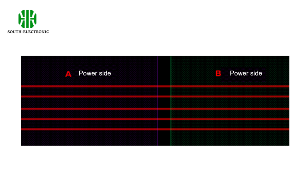
What are the effects of "cross-split"?
Cross-split may not be relevant for low-speed signals, but in high-speed digital signal systems, high-speed signals use the reference plane as the return path, that is, the return path. When the reference plane is incomplete, the following adverse effects will occur:
a. It will cause discontinuous impedance of the routing;
b. It is easy to cause crosstalk between signals;
c. It will cause reflection between signals;
d. Increase the loop area of the current and the loop inductance, making the output waveform easy to oscillate;
e. Increase the radiation interference to the space, and be easily affected by the magnetic field in the space;
f. Increase the possibility of magnetic field coupling with other circuits on the board;
g. The high-frequency voltage drop on the loop inductance constitutes a common-mode radiation source and generates common-mode radiation through the external cable.
Therefore, PCB routing should be as close to a plane as possible and avoid cross-splits. If cross-splits are necessary or cannot be close to the power ground plane, these situations are only allowed in low-speed signal lines.
Handling of cross-splits in PCB design
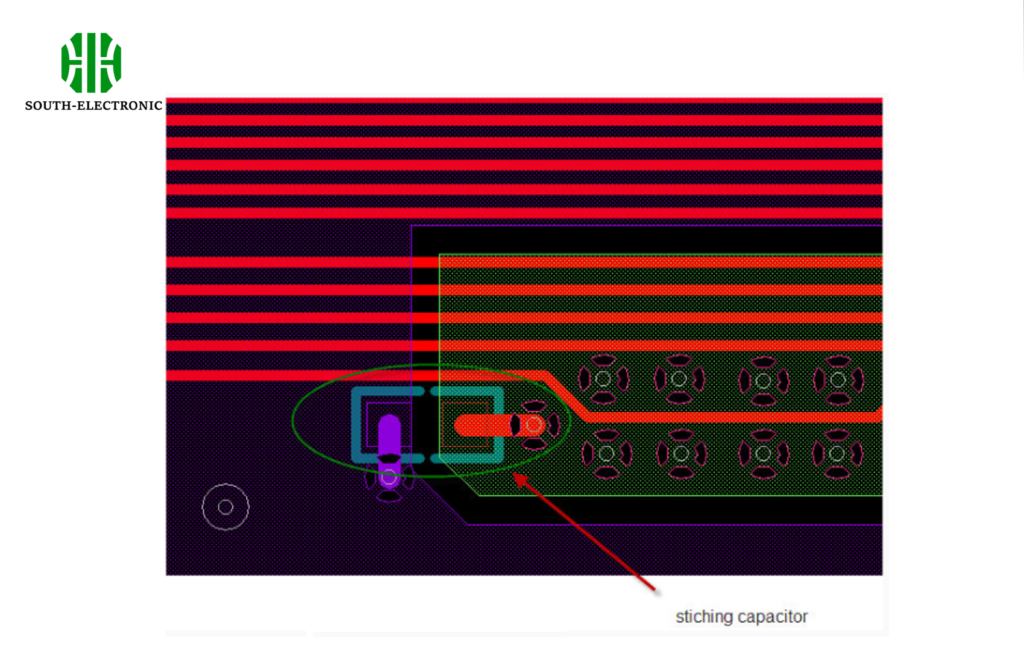
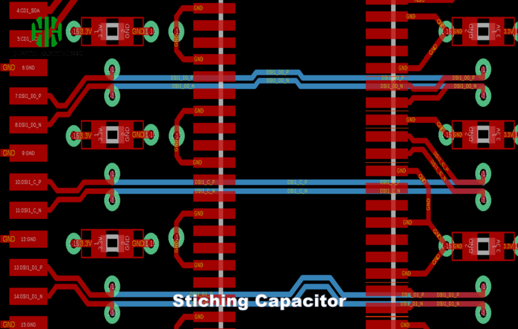
If cross-splits are inevitable in PCB design, how to deal with them? In this case, the splits need to be patched to provide a shorter return path for the signal. Common treatment methods include adding patching capacitors and cross-line bridges.
- Stiching Capacitor
Usually, a ceramic capacitor with a 0402 or 0603 package is placed at the signal cross-split, with a capacitance of 0.01uF or 0.1 uF. If space permits, you can add more such capacitors; at the same time, try to ensure that the signal line is within the 200mil range of the stitching capacitor, the smaller the distance, the better; and the networks at both ends of the capacitor correspond to the networks of the reference plane through which the signal passes, see the network connected at both ends of the capacitor in the figure below, two different networks highlighted in two colors:
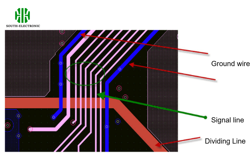
- Cross-line bridging
The common method is to "ground-enclose" the cross-split signal at the signal layer, or it may be the signal line of other networks. This "ground-enclosed" line is as thick as possible. For this processing method, refer to the figure below.
High-speed signal wiring skills
- Multilayer wiring
High-speed signal wiring circuits are often highly integrated and have high wiring density. The use of multilayer boards is both necessary for wiring and an effective means to reduce interference. Reasonable selection of the number of layers can greatly reduce the size of the printed board, make full use of the middle layer to set up shielding, better achieve nearby grounding, effectively reduce parasitic inductance, effectively shorten the transmission length of the signal, and greatly reduce cross-interference between signals.
- The fewer bends in the lead, the better
The fewer bends in the lead between the pins of high-speed circuit devices, the better. It is best to use full straight lines for the leads of high-speed signal wiring circuits. If a turn is required, a 45° fold line or arc turn can be used. This requirement is only used to improve the fixing strength of the steel foil in low-frequency circuits, but in high-speed circuits, meeting this requirement can reduce the external emission and mutual coupling of high-speed signals, and reduce signal radiation and reflection.
- The shorter the lead, the better
The shorter the lead between the pins of high-speed signal wiring circuit devices, the better. The longer the lead, the greater the distributed inductance and distributed capacitance, which will have a lot of impact on the passage of high-frequency signals in the system. It will also change the characteristic impedance of the circuit, causing reflection and oscillation in the system.
- The fewer the lead layer alternations, the better
The fewer the lead layer alternations between the pins of high-speed circuit devices, the better. The so-called "the fewer the lead layer alternations, the better" means that the fewer the vias used in the component connection process, the better. According to measurements, a via can bring about 0.5pf of distributed capacitance, resulting in a significant increase in the delay of the circuit. Reducing the number of vias can significantly increase the speed.
- Pay attention to parallel cross interference
High-speed signal routing should pay attention to the "cross interference" introduced by the close parallel routing of signal lines. If parallel distribution cannot be avoided, a large area of "ground" can be arranged on the reverse side of the parallel signal lines to greatly reduce interference.
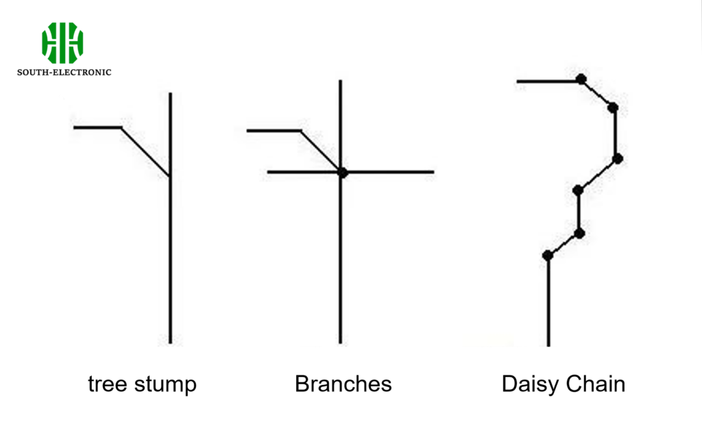
- Avoid branches and stumps
High-speed signal routing should try to avoid branches or stumps. Tree stumps have a great impact on impedance and can cause signal reflection and overshoot, so we usually avoid tree stumps and branches when designing. Using daisy chain wiring will reduce the impact on the signal.
- Try to run the signal line on the inner layer
High-frequency signal lines running on the surface are prone to generate large electromagnetic radiation and are also easily interfered by external electromagnetic radiation or factors. Route the high-frequency signal line between the power supply and the ground wire. Through the absorption of electromagnetic waves by the power supply and the bottom layer, the radiation generated will be greatly reduced.

