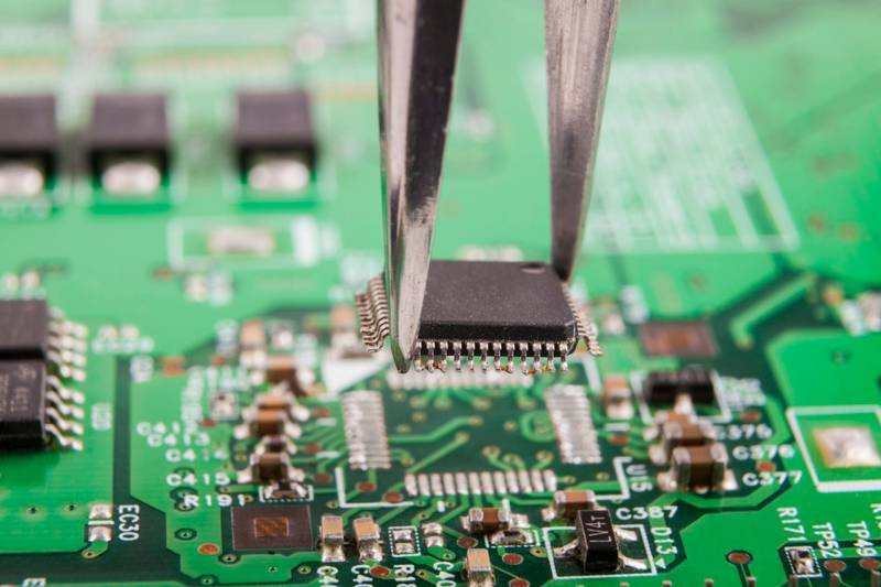
Ever built a circuit board that failed compliance tests? Your design might be leaking electromagnetic noise like a sieve. EMI isn’t just technical jargon—it’s the invisible saboteur hiding in your PCB.
EMI (Electromagnetic Interference)[^1] refers to disruptive electromagnetic noise in PCBs caused by high-speed signals, power fluctuations, or external sources. It distorts signals, causes data errors, and triggers overheating—issues resolved through layout optimization[^2], shielding, and EMC compliance measures.
)
EMI acts like static in a radio broadcast—but for your circuit board. To understand how this interference infiltrates your design, let’s dissect its causes, impacts, and control strategies.
Why Does EMI Occur in PCB Designs?
Watch your phone buzz near speakers—that’s EMI in action. But why does your carefully designed PCB emit this disruptive energy?
EMI arises from rapid signal switching (like clock circuits), improper grounding, component placement errors, and mismatched impedance in traces. These create unintended antennas radiating electromagnetic waves across frequencies from kHz to GHz ranges.
)
Three Root Causes and Solutions
| Source | Frequency Range | Radiation Type | Fix |
|---|---|---|---|
| Clock Signals | 1MHz-10GHz | Conducted | Guard Traces + Ferrite Beads |
| Power Planes | DC-100MHz | Radiated | Split Planes + Decoupling Caps |
| High-Speed Connectors | 500MHz-5GHz | Capacitive Coupling | Ground Shielding + Differential Pairs |
High-frequency signals (like USB 3.0’s 5Gbps data lines) act as unintended transmitters. I once debugged a medical sensor where a 25MHz oscillator disrupted ECG readings—adding ground planes reduced emissions by 12dB.
Current loops spanning large areas create magnetic dipoles. A poorly-routed 12V power trace in a motor driver became a 150MHz noise generator until we shortened the return path.
How Can EMI Impact Your PCB’s Functionality?
Your Wi-Fi drops when microwaves run? That’s EMI consequences 101. For PCBs, the effects are less visible but equally destructive.
EMI causes signal integrity loss[^3] (like USB packet errors), false sensor readings, processor lockups, and component overheating. In critical systems like avionics, it can trigger catastrophic failures through electromagnetic cascades.
)
Failure Modes by Severity Level
| Severity | Observed Effect | Typical Applications Affected |
|---|---|---|
| Critical | System reset/Data corruption | Medical devices, Automotive control |
| High | Communication errors >5% | Industrial PLCs, IoT gateways |
| Medium | Reduced SNR in analog circuits | Audio equipment, Sensors |
| Low | Minor timing skews (<1ns) | Consumer electronics |
I recall a drone controller where 2.4GHz WiFi interference caused motor ESC glitches. Shielding the RX module with copper tape dropped error rates from 18% to 0.3%.
VDD ripple from switching regulators can modulate RF circuits. A Bluetooth module’s range dropped 40% until we added LC filters—demonstrating how power-related EMI cripples functionality[^4].
EMI vs. EMC: What’s the Difference for PCBs?
Think of EMI as the crime and EMC as the law. One’s the problem, the other’s the solution.
EMI is unwanted electromagnetic noise, while EMC (Electromagnetic Compatibility[^5]) ensures devices operate without interfering/being interfered. PCBs achieve EMC via design rules suppressing EMI emissions/susceptibility to meet FCC, CE, or MIL-STD-461 standards.
)
Compliance Testing Framework
| Test Type | Purpose | Key Metrics |
|---|---|---|
| Radiated Emissions | Measure wireless EMI leakage | 30MHz-1GHz, <40dBµV/m @3m |
| Conducted Emissions | Test noise via power lines | 150kHz-30MHz, <66dBµV |
| Immunity | Check resistance to external EMI | Survives 10V/m field @80MHz |
| ESD | Verify discharge protection | Withstand ±8kV contact shocks |
Designing military-grade boards taught me EMC isn’t optional. A navy comms module failed radiated emissions at 868MHz—reshaping ground pours and adding feedthrough capacitors brought it within 6dB of spec.
Remember: Passing EMC tests requires anticipating EMI vectors during layout. I use 3D EM simulation tools[^6] like SIwave to predict hot spots before prototyping.
What Are the Most Common EMI Sources in PCBs?
Your board’s worst enemies might be components you specified. Here’s the rogue’s gallery of EMI generators.
Top EMI sources[^7] include crystal oscillators, switching regulators (like buck converters), high-speed digital interfaces (DDR, PCIe), and RF transceivers. Even "quiet" parts like LEDs can emit noise through improper dimming circuits.
)
Noise Source Analysis Matrix
| Component | Frequency Range | Coupling Method | Mitigation Technique |
|---|---|---|---|
| DC-DC Converter | 50kHz-5MHz | Conducted/Radiated | Snubber circuits, Shielding |
| DDR4 Memory Bus | 1.6GHz-3.2GHz | Crosstalk | Length Matching, Via Stitching |
| USB 3.2 Gen 2 | 10GHz | Differential Pair Radiation | Common Mode Chokes |
| WiFi Module | 2.4/5GHz | Antenna Radiation | Keep-Out Areas, Shielding Cans |
Never underestimate “low-speed” circuits. A 120Hz PWM-driven backlight induced audible noise in an audio codec via shared ground paths. Separating the power domains solved it.
Switching transients are brutal. A 2A step-down converter’s 100ns rise time created 30MHz ringing—adding a 22Ω resistor in series with the switch node dampened oscillations by 75%.
Conclusion
Controlling EMI requires understanding its sources, paths, and impacts. Through strategic layout, filtering, and shielding, engineers transform noisy boards into EMC-compliant marvels—one decoupling capacitor at a time.
[^1]: Understanding EMI is crucial for PCB design to prevent data errors and overheating. Explore this link for in-depth insights.
[^2]: Layout optimization is key to minimizing EMI. Discover effective strategies and techniques to enhance your PCB designs.
[^3]: Understanding how EMI affects signal integrity is crucial for designing reliable PCBs. Explore this link for in-depth insights.
[^4]: Discover the impact of power-related EMI on device performance and how to mitigate these issues for better reliability.
[^5]: Learn about EMC and its significance in ensuring your PCB operates effectively without interference. This knowledge is vital for engineers.
[^6]: Explore advanced simulation tools to predict and mitigate EMI issues before prototyping, enhancing design efficiency.
[^7]: Understanding EMI sources is crucial for effective design and mitigation strategies in PCB development.