
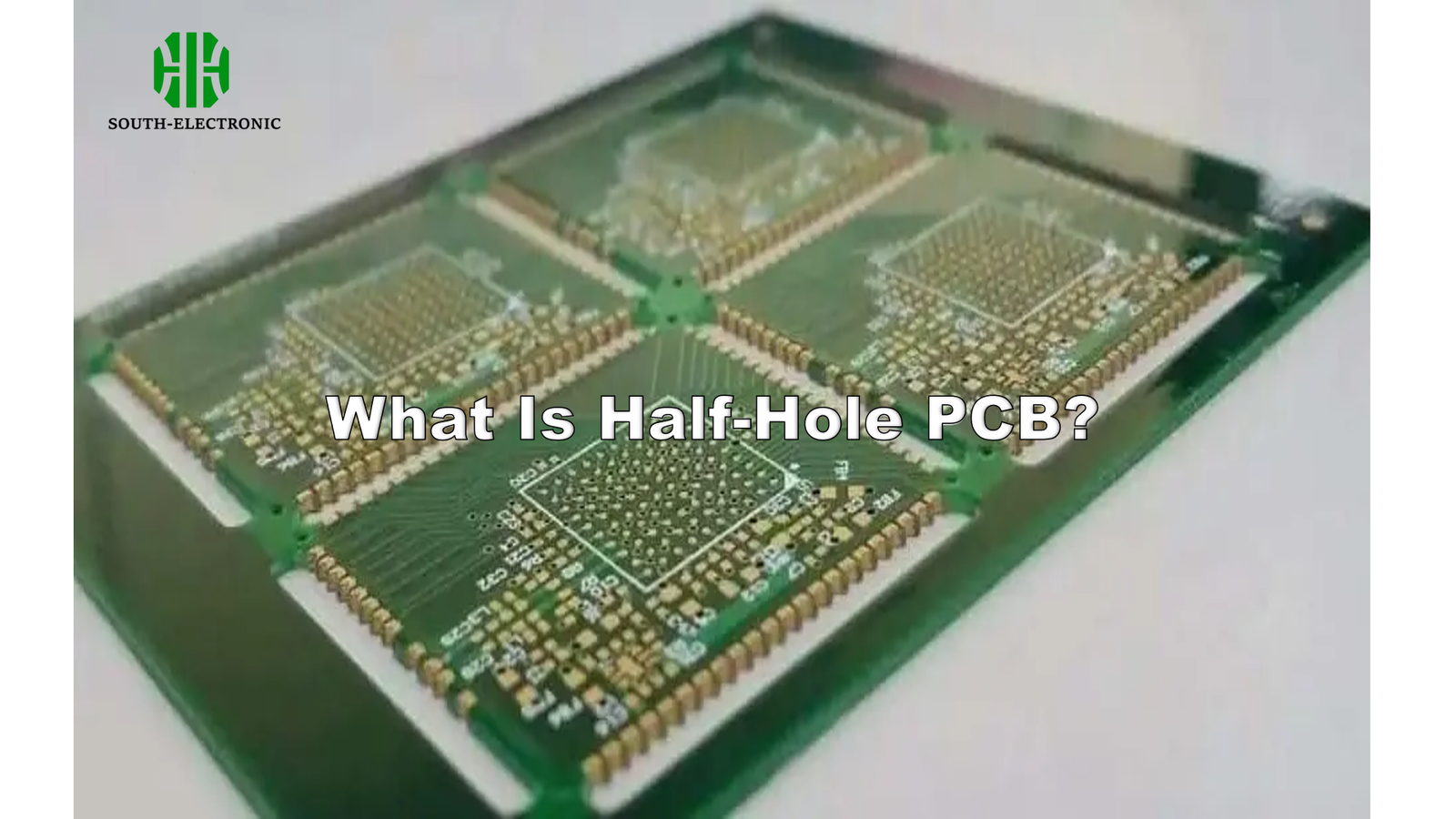
Ever struggled with bulky PCB stacking in high-density electronics? Traditional vias limit design flexibility and eat up space. Half-hole PCBs solve this with elegant metallized edges that act as both structural anchors and electrical bridges.
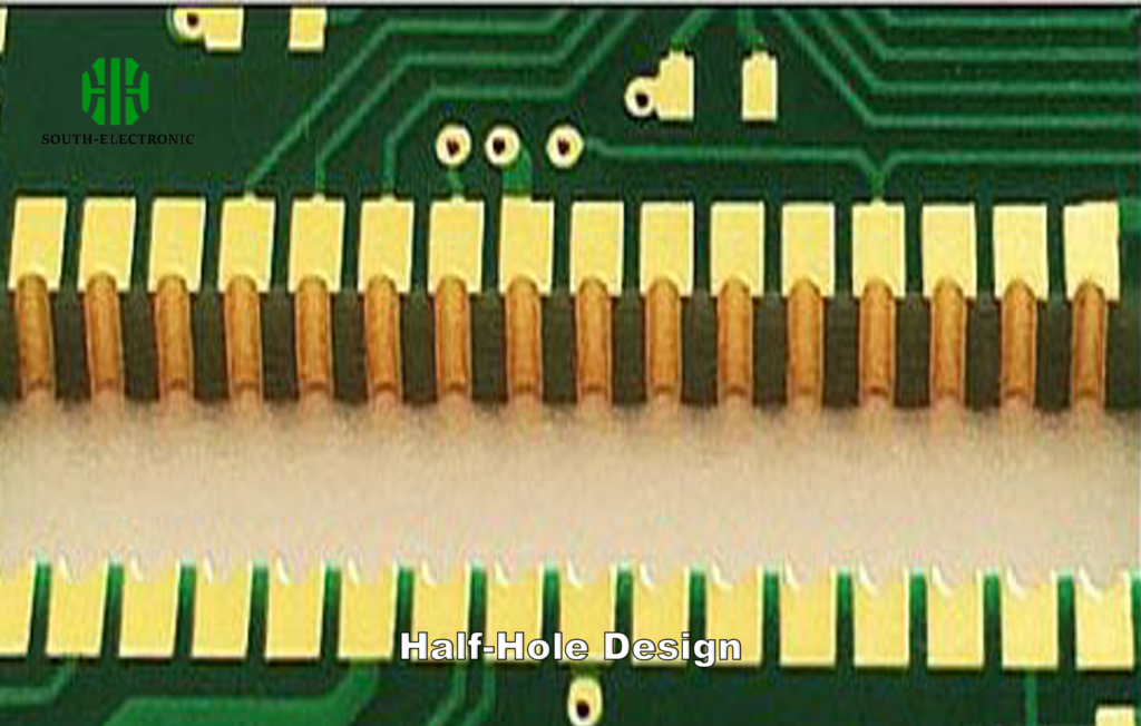
Half-hole PCBs[^1] use semicircular plated cavities along board edges to enable vertical stacking and multi-board interconnects while maintaining mechanical stability. They’re critical for 5G modules[^2] and IoT devices where space and reliability collide.
Now that you know what they are, let’s dissect their pros/cons, design nuances, and why they’re replacing standard vias in cutting-edge tech. By the end, you’ll see why engineers either love or fear them.
What Are the Advantages and Disadvantages of Half-Hole PCB?
One client insisted half-holes would solve their drone’s signal loss issues—until thermal stress cracked the boards. Like any tool, they shine only when applied correctly.
Advantages: Space-efficient stacking, 15-20% greater connection density vs. standard vias, vibration resistance[^3].
Disadvantages: 30% higher fabrication costs, 500 cycle durability.

Breaking Down the Tradeoffs
Let’s strip away the marketing hype:
| Pros | Cons | Mitigation Strategies |
|---|---|---|
| 50% space reduction | $2.15/board vs $1.50 | Use for high-margin products |
| MIL-STD-202 shock compliant | Limited to 4-layer designs | Pair with HDI substrates |
| 20% faster assembly | Requires laser drilling | Avoid manual depaneling |
I’ve seen teams ruin batches by using standard carbide drills—laser etching is non-negotiable. For automotive ECUs, the vibration resistance justifies the cost. Consumer gadgets? Often overkill.
What Are the Key Points in the Design of Half-Hole PCB?
Designing half-holes feels like threading a needle blindfolded. Miss by 0.01mm, and the board fails FCC emission tests.
Ensure 0.2mm clearance between hole edge and traces, use 35μm copper plating, and avoid placing half-holes near flex zones. Always simulate thermal cycling[^4] (ΔT ≥ 100°C) beforehand.
The 4 Non-Negotiables
-
Material Matters
- FR-4 cracks under repeated thermal stress. Use polyimide or Rogers 4350B for >500 cycle durability.
- ⚠️ Avoid lead-free HASL—go for ENIG or immersion silver to reduce pit corrosion.
-
Fabrication Checks
| Parameter | Target |
|---|---|
| Drilling diameter | 0.3mm ±0.03mm |
| Plating thickness | ≥25μm |
| Aspect ratio | ≤8:1 |
-
Panelization
- Use v-scoring, not tab routing, to prevent uneven stress during depaneling.
-
Testing
- Perform 72-hour HAST (Highly Accelerated Stress Test)[^5] at 130°C/85% RH.
Skip any step, and you’ll face intermittent connections in field devices. I learned this after a medical IoT recall traced back to under-plated half-holes.
Why Choose Half-Hole Instead of Standard PCB Vias?
Standard vias work until you need aerospace-grade reliability in a smartwatch. Half-holes merge form and function where millimeters matter.
Choose half-holes for vertical board stacking[^6], ultra-compact wearables, or high-G environments. Standard vias remain better for cost-sensitive, low-density designs with minimal thermal cycling.
)
When to Use (and Avoid) Half-Holes
| Scenario | Half-Hole Fit? | Why? |
|---|---|---|
| 5G mmWave antennas[^7] | ✅ Yes | Minimize RF interference |
| Budget DIY projects | ❌ No | Costs outweigh benefits |
| Automotive sensors | ✅ Yes | Withstand engine vibrations |
| High-power LED arrays | ❌ No | Heat warps plated edges |
At a previous job, we cut a drone’s PCB footprint by 40% using half-hole stacking—but only after switching to aluminum-core boards to compensate for heat issues.
Conclusion
Half-hole PCBs unlock game-changing density and reliability in 5G/IoT devices but demand surgical precision in design and fabrication. Choose them when every micron and shock test matters.
[^1]: Explore the advantages of Half-hole PCBs to understand their role in modern electronics and how they can enhance design efficiency.
[^2]: Learn how 5G modules leverage Half-hole PCBs to improve performance and reliability in high-density applications.
[^3]: Discover why vibration resistance is crucial in PCB design, especially for automotive and high-performance applications.
[^4]: Thermal cycling is vital for assessing PCB durability. Learn more about its importance and methods to implement it effectively.
[^5]: HAST is essential for validating PCB reliability under stress. Discover its significance and how to conduct it properly.
[^6]: Learn how vertical board stacking can enhance PCB design efficiency and save space in compact devices.
[^7]: Discover the critical design considerations for 5G mmWave antennas to ensure optimal performance and minimal interference.

