What is the best IC packaging for PCB?
IC packaging refers to the material and method used to encase semiconductor devices and their connections in a protective enclosure that prevents damage and corrosion. IC packaging varies significantly in form, size, and functionality. The most popular IC package among designers and engineers is typically the Ball Grid Array (BGA) because of its superior performance, high density of interconnections, and efficient heat dissipation, which are crucial for advanced, high-performance electronics.
What are the types of IC packaging?
IC packaging can be categorized into several types based on their mounting style and the technology used. Major types include:
- Through-Hole Technology (THT): Pins of the IC are inserted through holes drilled into the PCB and soldered to pads on the opposite side.
- Surface Mount Technology (SMT): ICs are placed directly onto the surface of a PCB without through holes. Types include:
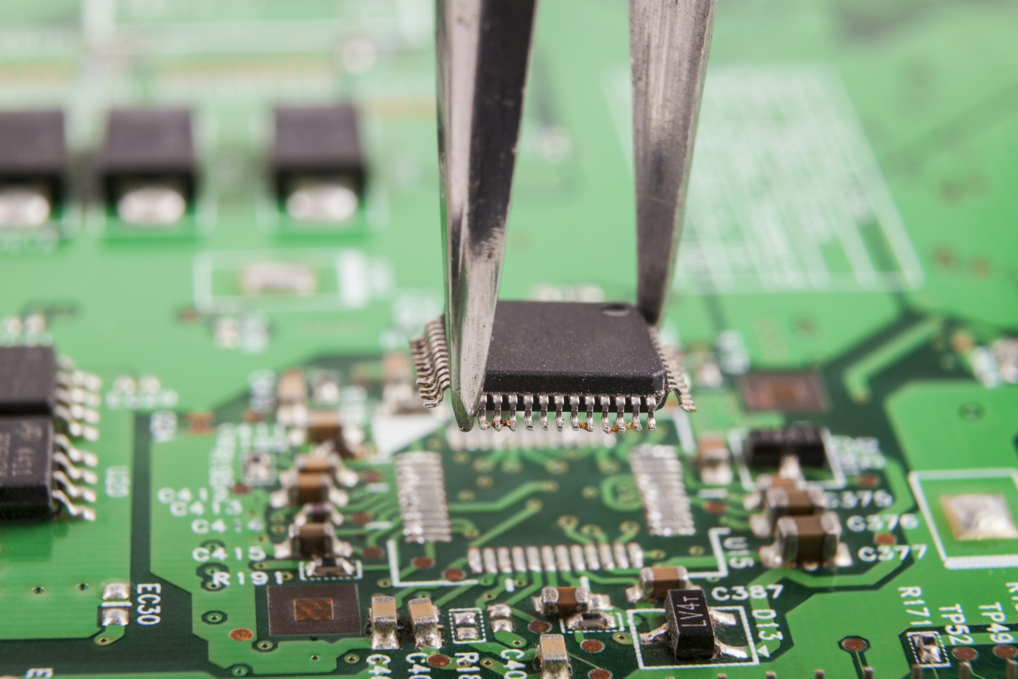
- Quad Flat Package (QFP): A rectangular package with leads on all four sides.
- Ball Grid Array (BGA): Uses an array of solder balls as connectors underneath the package, providing better performance at a higher density.
- Chip Scale Package (CSP): Similar in size to the chip itself, minimizing the footprint.
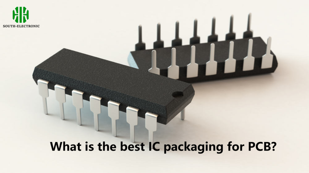
- Dual In-line Package (DIP): An older style, characterized by two parallel rows of pins.
- Advanced packages:
- System in Package (SiP): Contains more than one chip in a single package.
- Package on Package (PoP): Stacking of different semiconductor packages.

| Type | Characteristics | Common Uses |
|---|---|---|
| THT | Through-hole technology, sturdy, reliable | Industrial, automotive, and legacy systems |
| QFP | High pin count, square, flat | Complex high-density applications |
| BGA | Solder balls on the underside, high performance | High-performance computing, smartphones |
| CSP | Very small size, near chip-scale footprint | Mobile devices, portable electronics |
| DIP | Large, easy to handle, through-hole mount | Prototyping, educational kits |
| SiP | Multiple functional blocks in one package | Multifunctional devices, space-limited applications |
| SOP | Smaller than DIP, surface mount, rectangular package | Compact devices, general electronics |
How do I test different IC packages on a PCB for functionality?
Testing IC packages on a PCB for functionality generally involves several steps to ensure the ICs perform as expected in the circuit:
- Visual Inspection: Checking for physical damage, correct placement, and soldering defects.
- In-Circuit Testing (ICT): Using specialized equipment to test the electrical performance of components while integrated into a PCB.
- Functional Testing: Powering the PCB and testing its functionality through the intended operational conditions to ensure all components interact correctly.
- Automated Optical Inspection (AOI): Utilizing high-speed cameras and lighting to detect defects in component placement and soldering.
- X-ray Inspection: Employed especially for non-visible soldering like BGAs to check for alignment and quality of solder joints beneath the IC package.
Each type of test is crucial to ensure that the ICs are functioning correctly in their respective applications and can help in early detection of potential failures.

How does the choice of IC packaging affect PCB reliability?
- Thermal Management: Packages with better heat dissipation protect the IC and the PCB from overheating, enhancing overall reliability.
- Signal Integrity: Shorter and more efficient interconnects in certain packages ensure stable and clear signal transmission, crucial for high-performance applications.
- Mechanical and Environmental Protection: Sturdy packaging choices improve mechanical stability and offer better protection against environmental hazards, increasing the PCB’s durability in challenging conditions.
The choice of IC packaging affects PCB reliability through its impact on thermal management, mechanical stability, signal integrity, the manufacturing process, size, weight, and environmental protection. Each application might prioritize these factors differently, guiding the choice of the most appropriate IC packaging for reliability.


