
As devices shrink but capabilities expand, traditional circuit boards hit physical limits. IC PCBs solve this paradox through revolutionary integration – but what exactly makes them different?
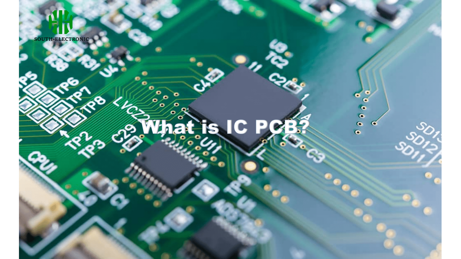
An IC PCB[^1] (Integrated Circuit Printed Circuit Board) combines semiconductor chips and standard PCB traces into one substrate. Unlike conventional boards, this fusion enables ultra-dense interconnections while maintaining signal integrity – critical for 5G phones, implantable medical devices, and edge AI systems.
Let’s dissect four key aspects that make IC PCBs both fascinating and complex – starting with their fundamental architecture.
What Exactly is an IC PCB and How Does It Differentiate from Regular PCB?
Imagine printing microchips directly onto circuit boards instead of soldering them. That’s IC PCB’s core innovation – but the implementation details matter most.
An IC PCB integrates bare semiconductor dies into the PCB substrate using embedded wafer-level packaging[^2]. This eliminates 97% of solder joints found in traditional PCB assemblies, reducing failure points while doubling connectivity density.
)
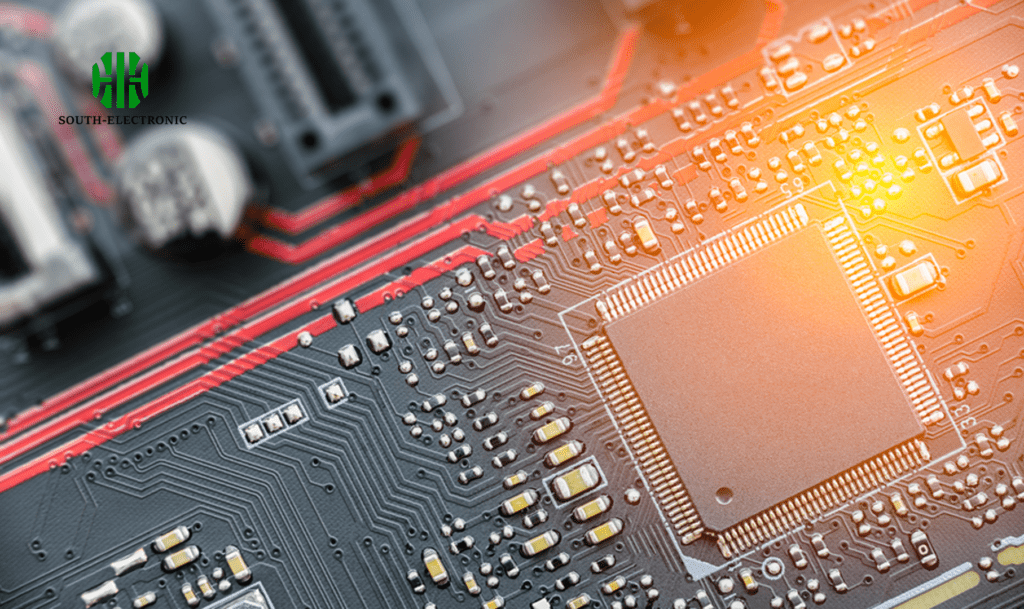
Structural Breakdown
Three key differences define IC PCB architecture:
| Feature | Regular PCB | IC PCB |
|---|---|---|
| Component Mounting | Surface-soldered chips | Embedded bare dies |
| Interconnect Density | 100-200 traces/cm² | 500-1000 traces/cm² |
| Signal Path Length | 2-5mm between chips | 0.1-0.5mm intra-layer |
Material Innovation
IC PCBs use modified FR-4 with 34μm ultra-thin dielectric layers, allowing microvias with 50μm diameters. This supports 10Gb/s+ signal speeds versus 1Gb/s limits in conventional boards.
Thermal Management
Embedded chips transfer heat through copper-filled thermal vias directly to aluminum nitride heat spreaders. This achieves 15°C lower operating temps than surface-mounted QFN packages.
Manufacturing Process
Unlike traditional pick-and-place assembly, IC PCB production involves:
- Laser-drilled cavity formation
- Die attach with conductive epoxy
- Sequential build-up lamination
- Direct laser structuring of traces
Why Are IC PCBs Crucial for Modern Electronics Design?
When Apple’s latest watch added blood glucose monitoring, space constraints forced radical redesigns. IC PCBs made it possible – here’s why they’re indispensable.
IC PCBs enable 60% smaller footprints than conventional boards while handling 10x more I/O connections. This allows wearable devices[^3] to incorporate advanced biosensors without compromising battery size or processing power.
)
Applications Driving Adoption
High-Density Requirements
- Smartphones: 5G mmWave antenna arrays need 0.2mm pitch interconnects
- Neural implants: 512-channel brain-machine interfaces
- Automotive radar: 77GHz transceivers with zero parasitic capacitance
| Performance Metrics | Parameter | IC PCB Advantage |
|---|---|---|
| Signal Loss | 0.3dB/cm @ 10GHz vs 1.2dB | |
| Crosstalk | -45dB vs -28dB | |
| Power Integrity | 5mV ripple vs 50mV |
Case Study: A drone flight controller using IC PCB achieved:
- 40% weight reduction
- Triple gyro sampling rate
- 2x longer flight time
Key Design Considerations: How to Optimize IC PCB Layout?
An engineer once ruined $200k of IC PCBs by overlooking thermal expansion rates[^4]. Learn from such mistakes with these critical guidelines.
Optimal IC PCB layout requires co-designing semiconductor die placement with high-speed routing channels. Key factors include matched Dk values across materials, controlled impedance from first principles, and hybrid HDI stackup planning.
Layout Optimization Matrix
| Challenge | Solution | Tool Example |
|---|---|---|
| Signal Integrity | 3D field solver analysis | Ansys HFSS 3D Layout |
| Power Distribution | Buried capacitance layers | Thin core CCL-HD |
| Thermal Stress | Coefficient-matched adhesives | Henkel ABLIS HR |
| DFM Compliance | Real-time DRC checks | Cadence Allegro Constraint Mgr |
Material Selection Flow
- Start with Tg (Glass Transition Temp): ≥170°C for lead-free reflow
- Match CTE: 6-8 ppm/°C to silicon dies
- Confirm Dk/Df stability across frequency bands
Rule of Thumb: All high-speed traces should follow the 3W rule (trace separation = 3x trace width) to prevent crosstalk.
What Should You Look for When Choosing an IC PCB Manufacturer?
"When factories cut corners on embedded die alignment, entire batches become RFID tags that can’t be read." First-hand experience shapes these selection criteria.
Choose manufacturers with ISO-9001 and IATF-16949 certifications[^5], 10+ years of IC PCB experience[^6], and ≤5μm placement accuracy. Verify their R&D investments – leaders spend 8-12% revenue on advanced packaging R&D[^7].
)
Vendor Qualification Checklist
| Factor | Benchmark | Verification Method |
|---|---|---|
| Yield Rate | ≥98% for 8-layer IC PCB | Audit final test reports |
| Tooling Capabilities | Laser drills ≤30μm | Request demo board |
| Material Bank | 5+ certified substrates | Review supplier list |
| Turnaround Time | 10-day standard lead | Compare multiple quotes |
Hidden Cost Drivers
- Panel utilization (aim for ≥85%)
- Test coverage (boundary scan mandatory)
- Via fill consistency (microsection analysis)
Always request:
- Reliability test data (1000 thermal cycles @ -55°C/+125°C)
- Cross-sectional samples
- 3rd-party material certifications
Conclusion
IC PCBs enable unprecedented electronic miniaturization through die embedding and ultra-HDI techniques. Mastering their design and manufacturing realities separates cutting-edge products from obsolete ones.
[^1]: Explore the advantages of IC PCBs to understand their revolutionary impact on modern electronics and their applications in various industries.
[^2]: Learn how embedded wafer-level packaging enhances PCB performance, reducing failure points and increasing connectivity density.
[^3]: Discover the impact of wearable devices on health monitoring and how they integrate advanced technology for better outcomes.
[^4]: Learn about the critical role of thermal expansion in PCB design to avoid costly mistakes and ensure reliability.
[^5]: Understanding these certifications can help you choose a reliable IC PCB manufacturer, ensuring quality and compliance.
[^6]: Experience in IC PCB manufacturing can significantly impact product quality and reliability, making it crucial for your selection process.
[^7]: Exploring R&D investments reveals how manufacturers innovate and improve their processes, which is vital for cutting-edge technology.


