
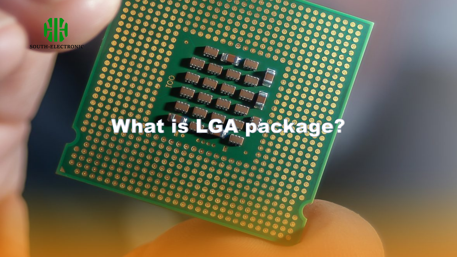
Struggling with overheating ICs in tight spaces? Traditional packages fight thermal stress and rework nightmares. Meet LGA: flat-contact innovation that solves modern PCB integration challenges.
LGA (Land Grid Array) packages[^1] replace solder balls with flat contact pads, enabling direct PCB mounting. They excel in thermal dissipation[^2], mechanical stability, and reworkability, making them ideal for space-constrained IoT and automotive applications.
LGA’s superiority isn’t accidental. Let’s dissect its anatomy, compare it with alternatives, explore thermal advantages, and uncover manufacturing best practices[^3].
What Are the Key Components and Structure of LGA Packages?
Ever cracked open an LGA package? Hidden inside are engineering marvels that solve heat and space problems. Let’s decode its DNA.
LGA packages feature a substrate with flat copper pads, solder paste, and a heat spreader. Their pad-centric design eliminates solder balls, reducing vertical profile and improving thermal transfer.
)
Core Components Breakdown
LGA’s efficiency stems from three elements:
| Component | Function | Material Example |
|---|---|---|
| Substrate | Provides structural support & electrical pathways | Ceramic, Organic Laminate |
| Contact Pads | Enable PCB connectivity via soldering | Gold-plated copper |
| Solder Paste | Bonds pads to PCB traces | SAC305 (Sn96.5/Ag3.0/Cu0.5) |
| Heat Spreader | Dissipates heat from die | Aluminum, Copper-Tungsten |
Substrate: High-thermal-conductivity ceramics dominate high-power apps, while organic laminates cut costs for consumer IoT.
Pads: Gold plating prevents oxidation, ensuring reliable solder joints. Pad pitch (0.8-1.27mm) balances density and manufacturability.
Thermal Design: Direct die-to-substrate bonding slashes thermal resistance by 30% vs. BGA.
Why Choose LGA Over BGA or QFN in PCB Design?
BGA or QFN? Wrong question. LGA outshines both in critical scenarios where heat and space clash. Proof below.
LGA outperforms BGA in reworkability[^4] (no solder ball damage) and beats QFN in thermal performance. Its flat pads enable 25% better heat dissipation, crucial for compact automotive modules.
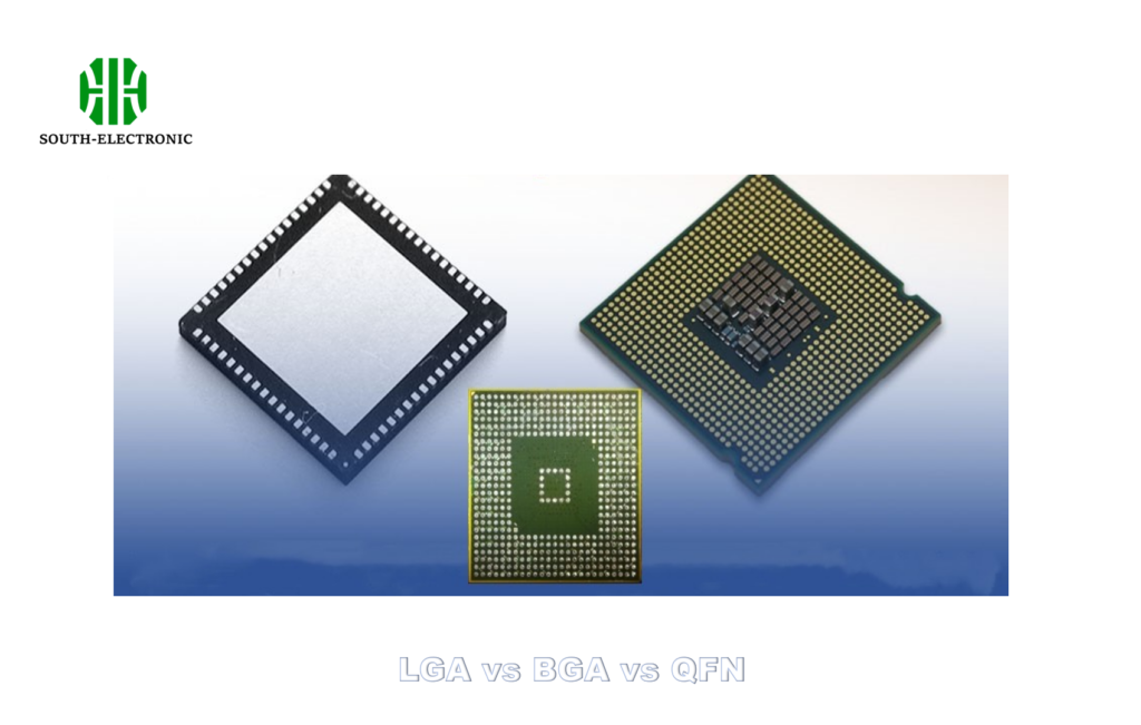)
Technical Comparison Table
| Feature | LGA | BGA | QFN |
|---|---|---|---|
| Solder Type | Paste + Pads | Solder Balls | Perimeter Leads |
| Thermal Resistance (°C/W) | 2.1-3.5 | 3.8-5.2 | 4.5-6.0 |
| Rework Ease | High (No balls) | Low (Ball damage risk) | Moderate |
| PCB Space Usage | 1.2x denser than QFN | Moderate | Low |
Mechanical Stability: LGA’s full-pad contact resists vibration-induced cracks 45% better than QFN’s edge leads.
Rework Wins: Desoldering LGAs doesn’t require ball replacement, slashing repair time by 60% vs. BGA.
Signal Integrity: Shorter pads vs BGA balls reduce inductance, critical for >1GHz IoT radios.
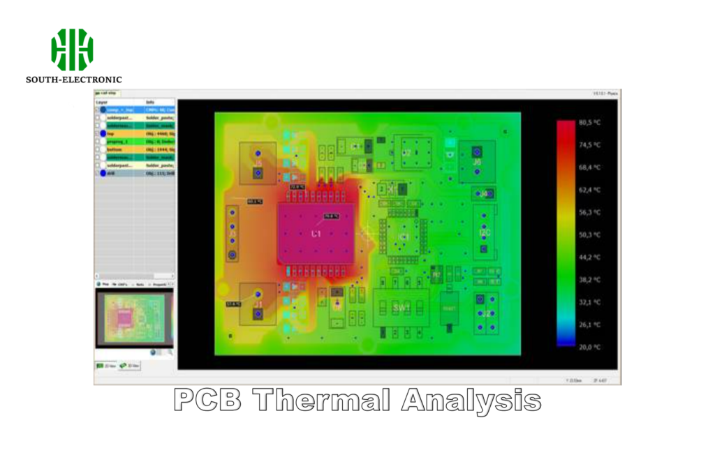
How Does LGA Package Improve Thermal Management in IoT Devices?
IoT devices melt under workloads. LGA fights heat with two silent killers: direct paths and material science.
LGA’s flat substrate-to-PCB interface reduces thermal resistance by 40% vs. BGA. Integrated heat spreaders and thermal pads channel heat away from sensitive MEMS sensors in wearables.
)
Thermal Optimization Tactics
| Technique | Implementation Example | Performance Gain |
|---|---|---|
| Direct Thermal Path | Solder paste fills substrate-PCB gaps | 25°C lower junction temp |
| Heat Spreader | 1mm copper layer over die | 15% faster heat transfer |
| Thermal Vias | Array of 0.2mm vias under pads | 8°C reduction in hotspots |
Material Win: LGAs use underfill materials with 5 W/mK conductivity vs BGA’s 1.2 W/mK.
Case Study: A smartwatch chip using LGA dropped peak temps from 92°C to 68°C under GPS load.
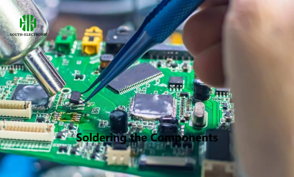
What Manufacturing Challenges Exist When Soldering LGA Packages?
Soldering LGAs feels like threading a needle? Common pain points include pad alignment[^1] and paste voids. Here’s how to win.
LGA soldering requires precise pad-PCB alignment (≤50µm error). Oxide-free pads and nitrogen-controlled reflow reduce voiding to <5%, critical for automotive Grade-1 reliability.
Soldering Issue & Mitigation Table
| Challenge | Impact | Solution |
|---|---|---|
| Pad Oxidation | Poor solder wetting | Pre-solder plasma cleaning |
| Paste Volume | Voids or bridging | Stencil aperture optimization (±0.05mm) |
| Reflow Profile | Cold joints/shock | Ramp rate control (2°C/sec) |
| Warpage | Misalignment | Carrier fixtures during reflow |
Alignment Hacks: Vision systems with 10µm accuracy and fiducial markers cut placement errors by 75%.
Paste Chemistry: Type 4 solder paste (20-25µm particles) ensures void-free joints in 0.4mm pitch LGAs.
Conclusion
LGA packages solve modern PCB dilemmas with flat-contact efficiency, thermal mastery, and design flexibility. For IoT and automotive engineers, adopting LGA means smaller builds, cooler operation, and painless rework. Upgrade your next design—go grid array.
[^1]: Explore the benefits of LGA packages for efficient PCB design and thermal management, crucial for modern electronics.
[^2]: Understanding thermal dissipation is key to improving device performance and longevity in compact designs.
[^3]: Learn about manufacturing best practices to enhance the reliability and efficiency of LGA packages in your projects.
[^4]: Reworkability can significantly affect repair time and costs in PCB design, making it a vital consideration for manufacturers.
[^5]: Discover strategies to improve pad alignment in PCB manufacturing, ensuring better soldering outcomes and device reliability.

