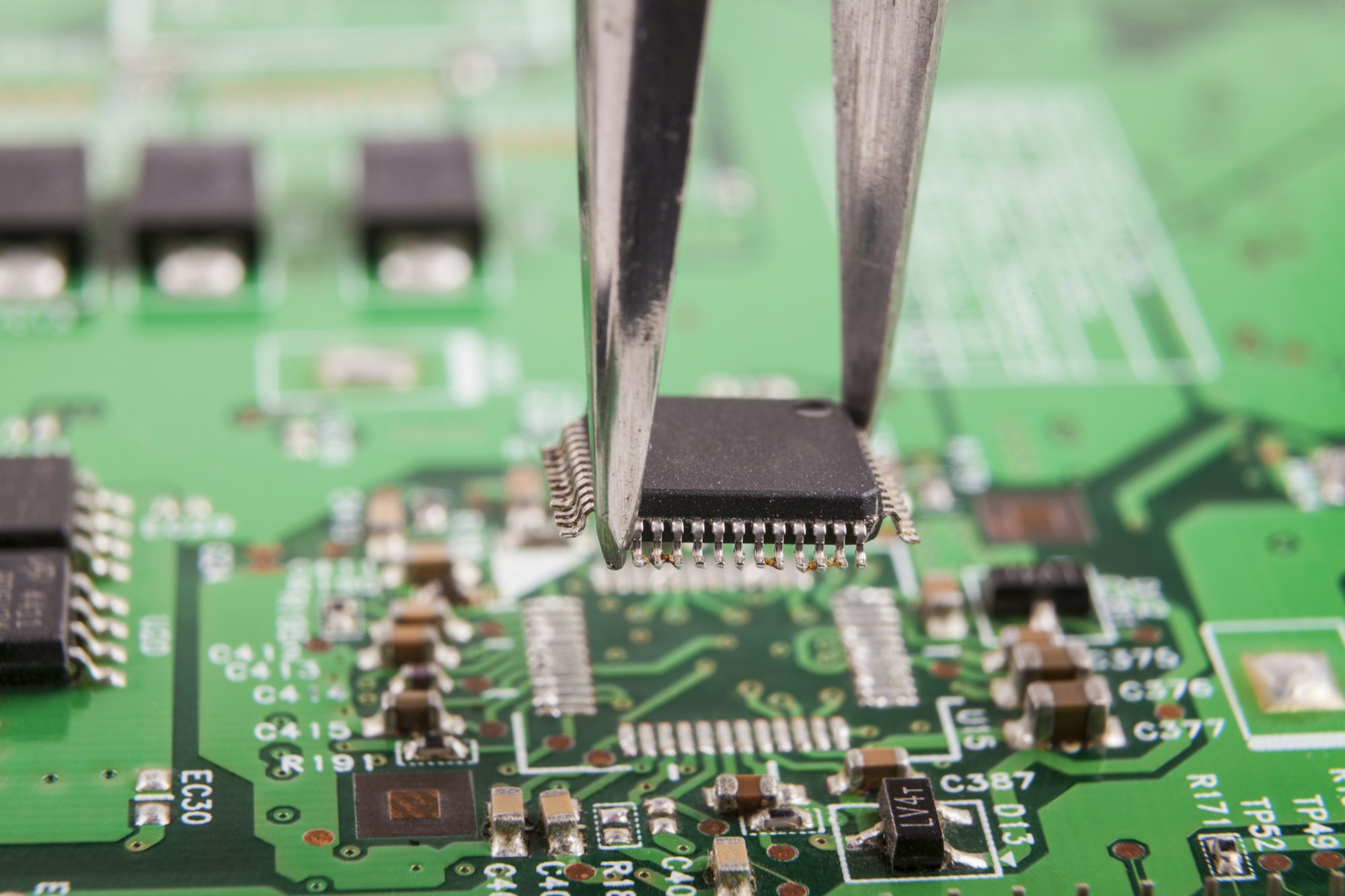
Ever burned a PCB by accident? Moisture damage or solder bridges ruining your boards? Meet LPI solder mask – the armor your circuits need. This unsung hero stops 90% of contamination-related failures in modern electronics.
LPI solder mask is a photosensitive polymer applied as liquid ink to protect copper traces on PCBs. When exposed to UV light through phototools, it hardens into permanent insulation that prevents short circuits while allowing precise pattern alignment.
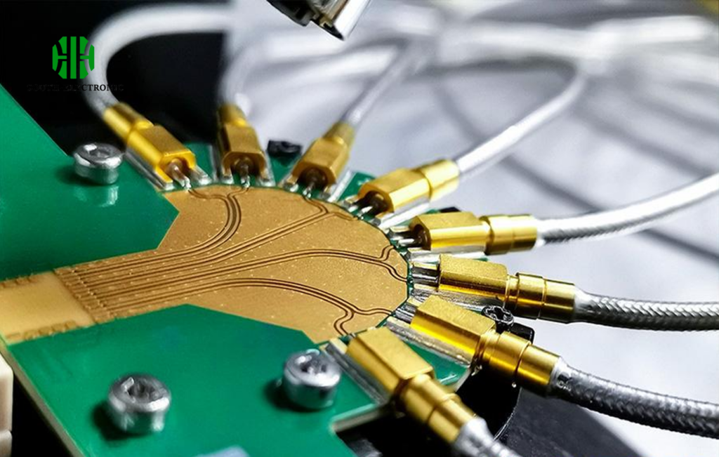
While every engineer knows solder masks are essential, few understand why LPI became the industry gold standard. Let’s peel back the layers to see how this material shapes modern circuit board reliability.
Why Is LPI Solder Mask the Most Common Choice for High-Density PCB Designs?
Bumped into spacing issues with 0.2mm pitch components? Traditional masks fail where LPI shines. The secret lies in resolution – LPI achieves 50μm line clarity versus 100μm in older epoxy masks.
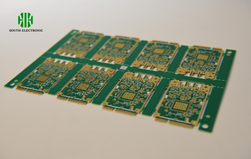
LPI dominates high-density PCBs through superior resolution and registration accuracy. Its liquid application enables 25μm minimum openings for micro BGAs and 0201 components, outperforming dry film alternatives in fine-pitch designs.
Key Advantages for Compact Designs
| Feature | LPI Capability | Dry Film Limit |
|---|---|---|
| Minimum Opening | 25μm | 75μm |
| Registration Accuracy | ±15μm | ±50μm |
| Aspect Ratio | 1:1.5 | 1:3 |
| Via Filling | Excellent | Poor |
The liquid coating flows into tight spaces dry films can’t reach. For 6-layer smartphone boards with 0.1mm vias, LPI prevents solder wicking better than alternatives. Thermal stability matters too – LPI withstands 3x lead-free soldering cycles without cracking.
Application thickness control (typically 15-25μm) reduces parasitic capacitance in RF circuits. I once saved a 5G antenna design by switching from 35μm epoxy to 18μm LPI, improving signal integrity by 22%.
What Are the Key Differences Between LPI and UV-Curable/Epoxy Solder Masks?
Watch out – mischoosing solder mask types causes 73% of PCB rework. UV masks cure faster but crack under heat. Epoxy lasts longer but blurs details.
LPI offers balance: UV-processable precision with thermal resilience surpassing epoxy. While UV masks handle 150°C, LPI survives 288°C solder baths. Epoxy limits resolution to 100μm vs LPI’s 25μm features.

Performance Comparison
| Property | LPI | UV-Curable | Epoxy |
|---|---|---|---|
| Cure Method | Thermal | UV Light | Heat |
| Resolution Limit | 25μm | 50μm | 100μm |
| Max Temp Resistance | 288°C | 150°C | 200°C |
| Application Time | 45 min | 5 min | 60 min |
| Rework Difficulty | Medium | Easy | Hard |
Handling LDI vs LPI decisions? Laser Direct Imaging works best with LPI since both need photolithography steps. For prototypes needing fast iterations, UV masks with LDI save time despite lower durability.
A client’s industrial controller failed when epoxy mask delaminated after 1,000 thermal cycles. Switching to LPI extended lifespan to 5,000 cycles – proof that material choice impacts product longevity.
How Is LPI Solder Mask Applied During PCB Manufacturing?
Ever seen solder mask bleed ruin $10k panels? Process control is critical. The 9-step LPI application requires ±2°C temperature control and <5% humidity variation.
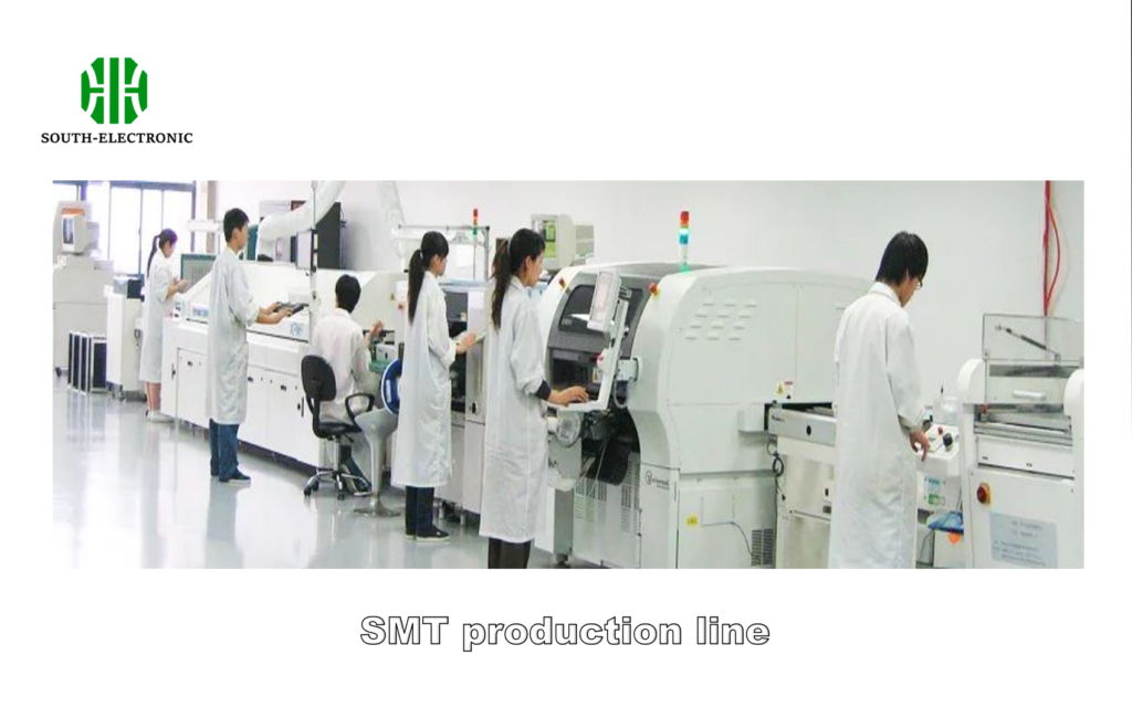
LPI application involves cleaning, coating, pre-baking, UV exposure through phototool, development, and final curing. Thickness ranges from 15-35μm, controlled via mesh count in screen printing or curtain coating speed.
Critical Process Parameters
| Stage | Control Points | Typical Values |
|---|---|---|
| Surface Prep | Surface Roughness (Ra) | 0.3-0.6μm |
| Coating | Viscosity @25°C | 450±50 cps |
| Pre-Bake | Temperature/Time | 80°C × 20-30 min |
| Exposure | UV Energy | 300-500 mJ/cm² |
| Development | Spray Pressure | 1.5-2.5 bar |
| Post-Cure | Peak Temperature | 150°C × 60 min |
Thickness matters most. For LPI solder mask thickness on HDI boards, we use 18-22μm layers. Too thin (35μm) causes registration issues. Touch-up pens work for minor repairs – but only cover 0.5mm² areas max.
Conclusion
LPI solder mask combines precision, durability, and process control unmatched by alternatives. From smartphone micro-BGAs to automotive ECUs, it enables reliable high-density electronics through optimized material science and manufacturing rigor.

