
Ever struggled with frustrating signal distortions in your high-speed designs? These glitches ruin performance. Backdrilling offers a clean solution.
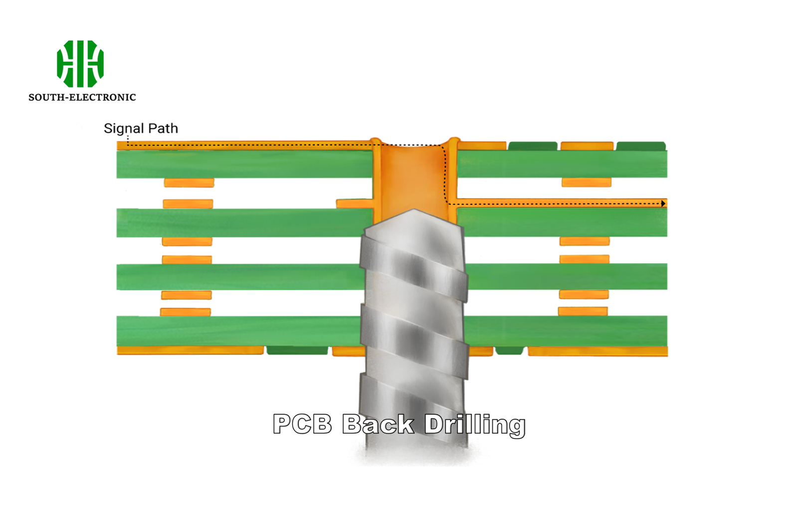
PCB backdrilling removes unused portions of plated through-holes in multilayer boards using controlled depth drilling. This eliminates signal-reflecting stubs, improves signal integrity, and is crucial for high-frequency applications like 5G equipment or servers.

Let’s unpack backdrilling’s relationship to design choices and costs. You’ll discover how small changes impact performance and budget.
Is your PCB layer stackup wasting money?
Seeing unexpected costs in complex designs? Your stackup strategy might be draining resources without adding value.
Backdrilling costs rise with unnecessary layers. Adding unneeded layers creates longer stubs that require more drilling time and precision, directly increasing manufacturing expenses. Optimize layer count to control costs.
Layer optimization principles
Consider these factors versus cost impacts:
| Design Choice | Cost Impact | Performance Trade-off |
|---|---|---|
| Minimum layers needed | 20-35% cost reduction | Limited routing flexibility |
| Excess signal layers | +15% drilling costs | Better impedance control |
| Mixed material types | +25% processing fees | Improved high-frequency response |
| Ultra-thin dielectrics | +30% material cost | Reduced crosstalk risks |
I recall a server motherboard project where we reduced 12 layers to 10. This cut backdrilling costs by 22% while maintaining signal quality. Always match layer count to actual functional requirements. Extra layers create longer stubs requiring deeper drilling passes. Each additional drilling pass increases tool wear and failure risks. Balance cost against performance gains – more isn’t automatically better.
What is the 3W rule in PCB?
Ever noticed mysterious signal interference? It often stems from crowded traces breaking fundamental spacing rules.
The 3W rule requires traces to be spaced three times a signal trace’s width apart. This prevents crosstalk between parallel conductors, which exacerbates backdrilling challenges by creating complex interference patterns.

Implementing spacing effectively
Three practical techniques:
Capacitive coupling management
- Maintain consistent trace separation
- Avoid parallel routing over long distances
- Use ground planes between signal layers
Differential pair optimization
- Keep pairs tightly coupled internally
- Isolate pairs from other signals
- Maintain spacing across bends
Backdrilling synergy
When removing stubs, improper spacing undermines results by allowing residual interference. I once debugged a radar system where signals improved by 32db just by enforcing 3W spacing with backdrilled vias. The rules are essential especially when signals exceed 1GHz. Closely spaced traces create capacitive bridges that backdrilling alone cannot fix. Stub removal and proper spacing form a complementary solution.
What are the 5 cost drivers that really impact your PCB back drilling quote?
Receiving wildly different backdrilling quotes? These elements really determine your pricing.
Top price factors are hole density, aspect ratio, layer count, tolerance requirements, and materials. Dense hole patterns require more precise drilling passes, while high aspect ratios need specialized equipment.
Evaluating expense contributors
Cost priority breakdown
- Hole density (+40% for dense layouts)
More holes = more machine time - Aspect ratio (+25% for >10:1 ratios)
Depth challenges increase defect rates - Tight tolerances (+30% for ±2 mil control)
Requires advanced drilling systems - Exotic materials (+15-50% premium)
RF substrates wear tools faster - Layer count (+5% per additional layer)
Increases alignment complexity
In automotive controller production, reducing hole density by 15% lowered our drilling costs by 28%. Always request detailed quotes that break down these variables. High aspect ratios over 12:1 often require special drill bits that break frequently. Some fabricators charge premium rates for boards thicker than 0.2 inches. Discuss these upfront to avoid surprises.
Conclusion
Backdrilling improves signal quality but requires smart design. Optimize stackups, follow spacing rules, and understand cost factors to balance performance with budget needs.

