What is PCB Etchback?
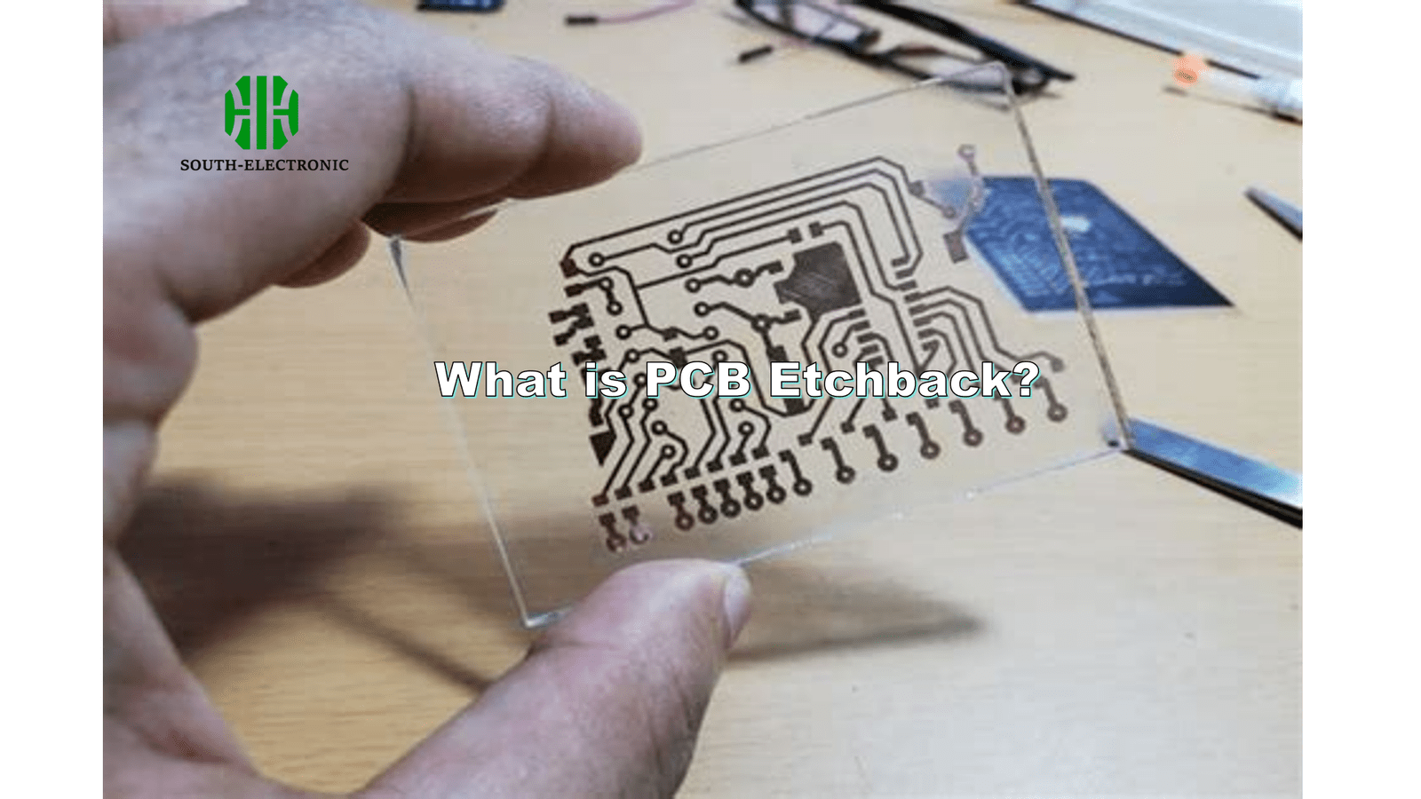
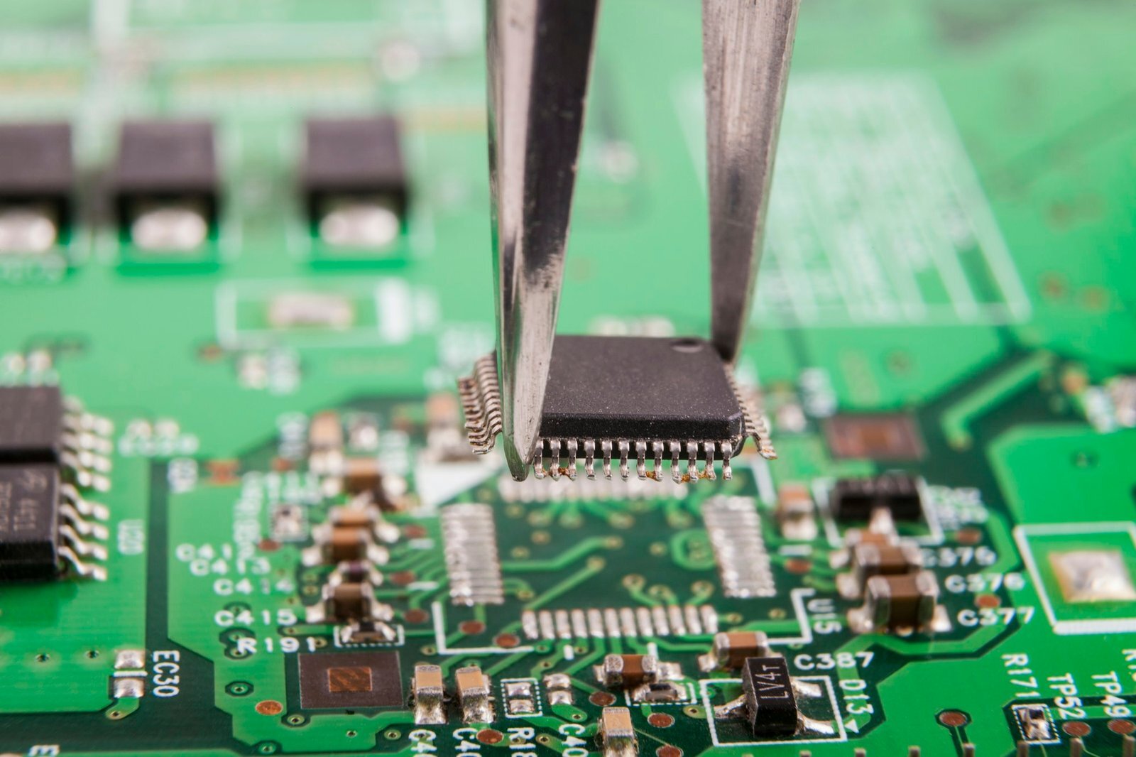
Etchback is a big deal in the making of multilayer printed circuit boards (PCBs). It’s the process of getting rid of extra copper or resin from the inside layers of the board, especially around the drilled holes. This makes sure the layers connect electrically, and that makes the PCB work better and last longer in all kinds of stuff.
Why is PCB Etchback Important?
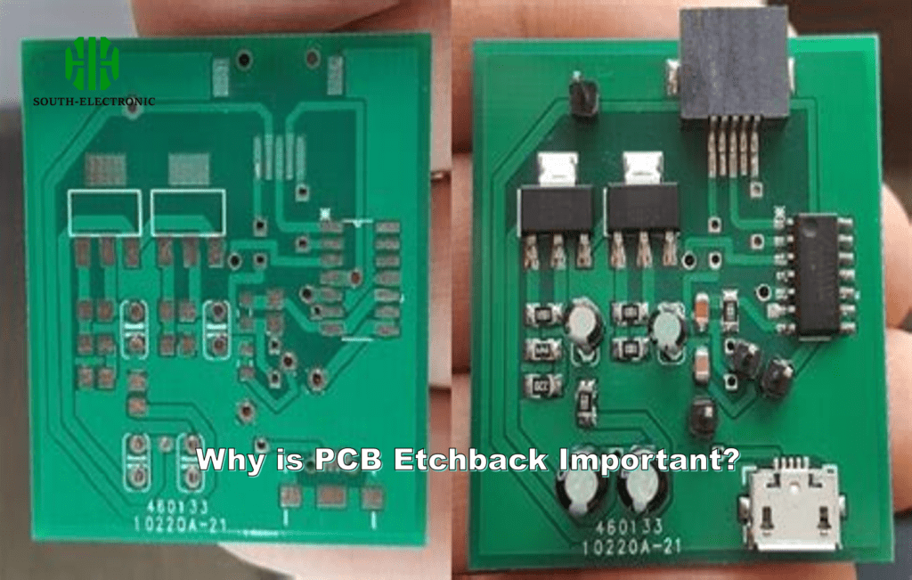
When you drill holes in multilayer PCBs, debris and resin can get inside them, which can mess up the electrical connections between the layers. PCB etchback gets rid of that crap, so the electricity can flow between the layers like it’s supposed to. That’s important for high-performance stuff like airplanes, the military, and medical devices.
How the PCB Etchback Process Works?
Step 1: Drilling of Vias
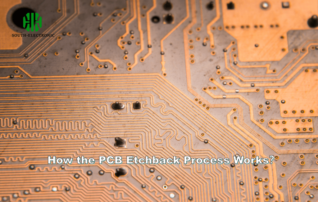
When you make a multilayer PCB, you have to drill holes to connect the different layers. But sometimes, resin gets in the holes and messes up the connection between the copper layers.
Step 2: Resin Removal
You have to get rid of the resin that gets on the sides of the holes when you drill them. This is important so that the copper layers inside the PCB can connect to each other and make a good electrical connection. You can clean the holes in different ways, like using chemicals or plasma. Each way has its own good and bad things, depending on how hard it is to make the PCB.
Step 3: Copper Exposure and Connectivity
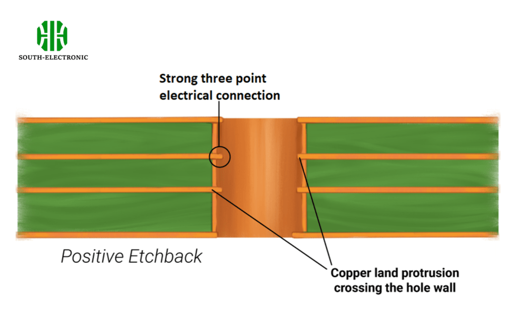
After you clean the holes, the copper layers inside the holes are all ready to go. This makes it easier for the layers to connect and makes the electrical connection between them better. If you’re making a PCB that needs to be really good, like for airplanes or the military, you have to make sure the copper connects in three places.
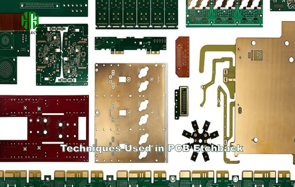
Techniques Used in PCB Etchback
1. Chemical Etching
Chemical etching involves the use of chemical solutions like potassium permanganate to dissolve the resin and expose the copper layers. While this method is effective, it requires careful handling of hazardous chemicals. Here’s an example of how chemical etching works:
| Chemical Solution | Target Material | Process Time | Effectiveness |
|---|---|---|---|
| Potassium Permanganate | Resin Smear | 20-30 minutes | High |
| Chromic Acid | Organic Material | 15-20 minutes | Moderate |
Advantages:
- Effective for large-scale production.
- Suitable for simple PCB designs.
Disadvantages:
- Requires careful chemical handling.
- Less precise compared to plasma etching.
2. Plasma Etching
Plasma etching is a more precise way of doing it. It uses ionized gas (plasma) to remove the resin without affecting the surrounding material. It works great on complex multilayer PCBs with tight tolerances.
| Plasma Gas | Etching Material | Precision Level | Applications |
|---|---|---|---|
| Oxygen | Organic Material | High | Complex PCBs |
| Fluorine | Copper Surface | High | High-reliability |
Advantages:
- High precision.
- Ideal for complex PCB designs.
Disadvantages:
- Higher cost.
- Requires specialized equipment.
Types of PCB Etchback
PCB etchback can be categorized into two primary types: positive etchback and negative etchback, each with unique characteristics.
1.Positive Etchback
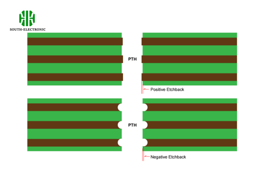
With positive etchback, the copper layers are fully exposed on all sides of the via hole. This creates a three-point connection between the internal copper layers, which enhances electrical performance and reliability. Positive etchback is ideal for high-reliability applications, but the aggressive nature of this technique can introduce stress into the PCB, potentially leading to cracks in the copper.
Key Features:
- Creates a three-point copper connection.
- Ensures robust electrical contact.
Best For:
- High-reliability PCBs (military, aerospace).
2.Negative Etchback
On the flip side, negative etchback recesses the copper layers from the edge of the via hole. This is a less aggressive approach and is often used in less demanding applications where the highest level of reliability isn’t required.
Key Features:
- Less aggressive process.
- Lower electrical performance compared to positive etchback.
Best For:
- Consumer electronics and lower-reliability applications.
Comparing Etchback and Desmear
Etchback and desmear are both processes aimed at cleaning via holes in PCBs, but they differ in how they achieve this goal.
| Process | Method | Purpose | Application |
|---|---|---|---|
| Etchback | Plasma or Chemical | Removes resin and exposes copper | High-reliability PCBs |
| Desmear | Chemical (Permanganate) | Removes smear only, no copper exposure | Less-critical applications |
Etchback is a critical step in making multilayer PCBs, especially for high-reliability industries like aerospace, defense, and medical devices. Whether you use chemical or plasma etching, etchback ensures clean, strong electrical connections between layers, which means better performance and reliability.

