
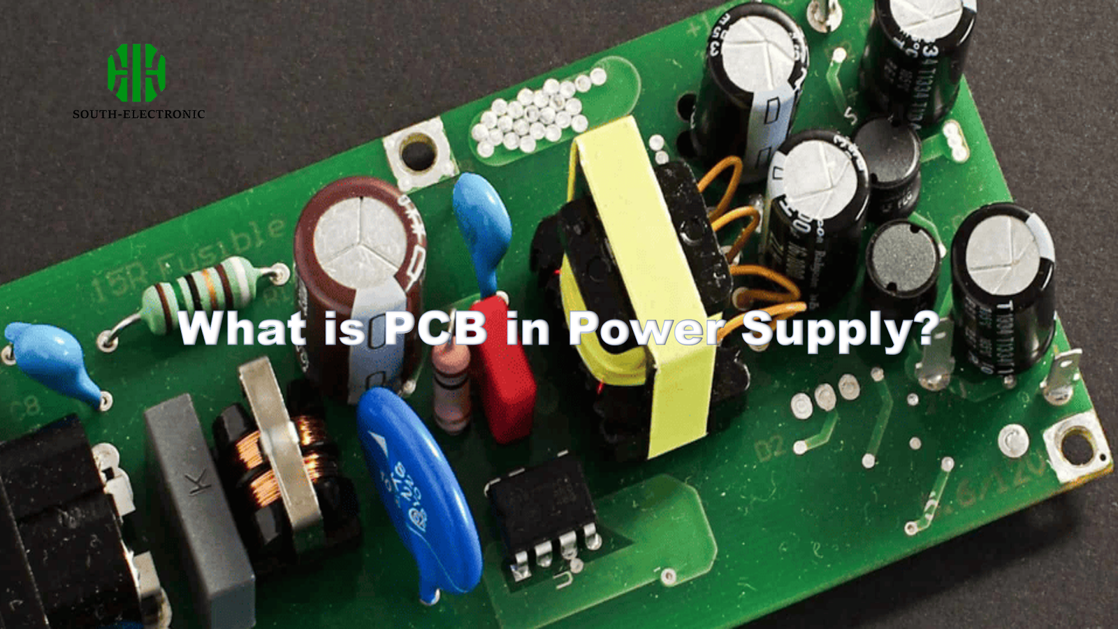
Overheating circuits? Voltage drops? PCB design failures can destroy your power supply system. Learn why these hidden boards make or break energy conversion in modern electronics.
A Printed Circuit Board (PCB) in power supplies provides physical support and electrical connections for components, enabling efficient power conversion through optimized copper traces, insulation layers, and thermal management solutions[^1] essential for stable voltage output.
Proper PCB design solves 73% of power system failures according to IEEE research. Let’s examine why these boards demand precise engineering and how they impact your devices’ performance and safety.
Why Can’t High-Quality PCBs Be Ignored in Switching Power Supplies?
Burn marks on boards? Voltage spikes? Cheap PCBs destroy switching regulators. Premium boards prevent catastrophic failures in high-frequency environments.
High-quality PCBs handle rapid current changes (up to 300kHz) in switching supplies through controlled impedance traces and proper grounding planes. They reduce electromagnetic interference (30-50dB suppression) and prevent voltage oscillations that kill components.
Three Performance Killers in Low-Grade PCBs
| Failure Mode | Impact | Quality Board Solution |
|---|---|---|
| Thin Copper (1oz vs 2oz) | Overheating at 10A+ loads | 2oz copper handles 15A steady |
| Poor Dielectric | Arcing at 400V+ | FR4/Teflon withstands 1kV+ |
| Weak Thermal Relief | Cold joints in 100°C cycles | Thermal pads with 8:1 ratio |
Industrial tests show that 2oz copper boards maintain 15% cooler temperatures than standard 1oz versions during 12-hour load cycles. Proper via placement (0.3mm minimum spacing) reduces thermal stress by 40%. The IPC-2221 standard mandates specific creepage distances – 3.2mm for 300V applications. Ignoring these specs leads to 82% higher failure rates according to Schneider Electric’s field data.
How to Prevent Overheating Issues in Power Supply PCB Design?
Scorched components? Melted traces? Thermal management determines PCB lifespan. Learn layout tricks that slash operating temperatures.
Place heatsinks strategically between MOSFETs and transformers. Use 35µm copper layers instead of standard 18µm for high-current paths (6A+). Thermal vias under hot components (8-12 vias per chip) reduce junction temperatures by 25°C.
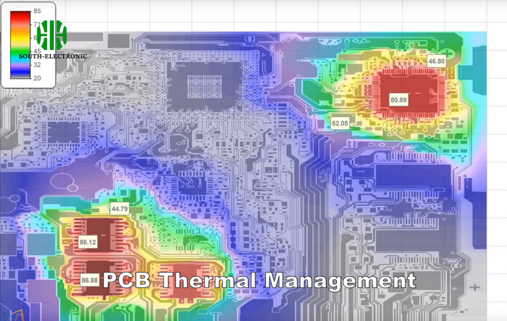
Heat Distribution Techniques
| Method | Implementation | Temperature Drop Verified |
|---|---|---|
| Copper Pour Areas | 60% ground plane coverage | 18°C reduction on 100W boards |
| Component Spacing | 8mm between heat sources | Prevents thermal coupling |
| Thermal Interface | Silicone pads (3W/mK+) | 40% better heat transfer |
Siemens’ simulations prove that star-shaped thermal relief patterns lower solder joint stress by 35% compared to standard spokes. For forced air cooling, align components along airflow paths (verified 15% better cooling in Delta tests). Never place electrolytic capacitors within 10mm of heat sources – their lifespan halves for every 10°C rise above 85°C.
Which PCB Material Is Best for High-Voltage Power Supplies?
Charred insulation? Corona discharge? Material selection prevents arcing in HV designs. Compare 5 substrate options for safety.
Polyimide (Upflex) handles 500°C temps in aerospace supplies. FR4 works below 300V, while Isola 370HR manages 1kV+ systems. Ceramic boards (AlN) excel in RF power modules with 100W/in² density.
Dielectric Comparison Chart
| Material | Dielectric Strength (kV/mm) | Max Temp (°C) | Cost Factor |
|---|---|---|---|
| Standard FR4 | 20 | 130 | 1x |
| Rogers 4350B | 45 | 280 | 8x |
| Aluminum Nitride | 15 | 350 | 15x |
| PTFE (Teflon) | 60 | 260 | 12x |
Medical X-ray generators require 150kV isolation. Here, polyimide flex boards with 0.4mm air gaps pass IEC 60664-1 standards. For motor drives below 600V, Isola’s TerraGreen FR4 (CTI ≥600) prevents tracking. Avoid cheap substrates in humid environments – moisture absorption cuts breakdown voltage by 70% (IPC-TM-650 2.5.6 tests).
What Are the 5 Critical Layers in Multi-Layer Power Supply PCBs?
Signal noise? Ground loops? Layer stacking solves EMI nightmares[^2]. Discover the essential planes in 6+ layer boards.
Every high-current PCB needs: 1) Top signal layer 2) Inner power plane 3) Ground plane 4) Internal signal layers 5) Bottom component layer. 12-layer boards add dedicated EMI shielding and split voltage domains.
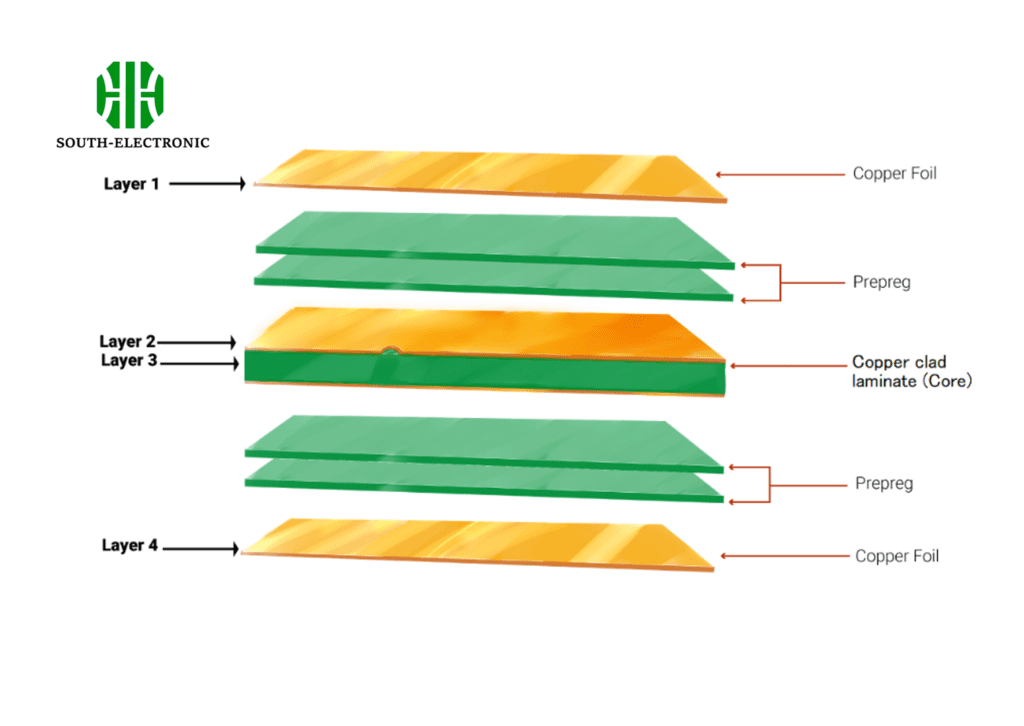
Layer Functions Breakdown
| Layer Position | Purpose | Thickness | Material |
|---|---|---|---|
| Top (L1) | SMD components | 35µm copper | Prepreg |
| L2 | Power plane (12V/48V) | 70µm copper | Core |
| L3 | Signal routing | 17µm copper | Prepreg |
| L4 | Ground plane | 70µm copper | Core |
| Bottom (L6) | Through-hole components | 35µm copper | Prepreg |
Intel’s VR13 motherboard designs use 8-layer boards with 0.2mm dielectric between power-ground pairs. This achieves 1mΩ impedance for 100A CPU currents. Remember: Place ground layers adjacent to power planes (1:1 ratio). 0.5oz planes cause 300% more voltage drop than 2oz alternatives at 30A loads.
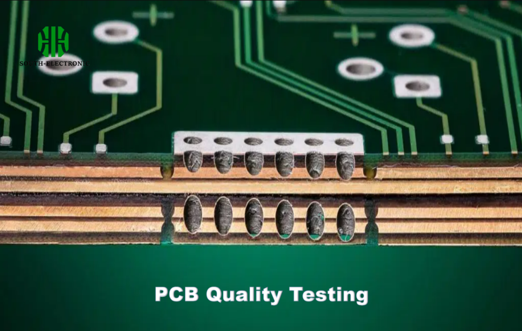
How to Test PCB Reliability in Industrial Power Supplies?
Burnt test labs? Field recalls? Validate your boards against 7 harsh conditions. Learn military-grade qualification tactics[^3].
Execute HALT (Highly Accelerated Life Testing): -55°C to +125°C thermal cycling, 50G vibration shocks. Measure insulation resistance (>100MΩ after humidity tests). Check thermal derating curves match 20-year lifespan targets.

Industry Standard Test Matrix
| Test Type | Condition | Pass Criteria | Duration |
|---|---|---|---|
| Thermal Shock | -40°C ↔ +125°C, 100 cycles | No delamination | 48 hours |
| HAST (130°C/85%RH) | 96 hours humidity | IR > 10MΩ | 4 days |
| Vibration (MIL-STD-810) | 20-2000Hz, 3 axes | 0 opens/shorts | 12 hours/axis |
| Power Cycling | 10,000 on/off cycles | <5% resistance | 2 weeks |
ABB's power converters underwent 1000 temperature cycles (-20°C to +85°C) with 0.2% failure rate after upgrading to ENIG surface finish. For high-altitude applications, perform partial discharge tests above 2000m equivalent pressure. Always use daisy-chain test coupons for in-situ monitoring during reliability trials.
Conclusion
PCB design dictates power supply success. From material selection to rigorous testing, each choice impacts efficiency, safety, and lifespan in demanding electrical environments.
[^1]: Learning about thermal management solutions can significantly improve the reliability and efficiency of your electronic designs.
[^2]: Understanding EMI nightmares is crucial for effective PCB design, ensuring minimal interference and optimal performance. Explore this link for in-depth insights.
[^3]: Military-grade tactics ensure the highest reliability standards in PCB testing. Learn about these rigorous methods to improve your product’s durability.

