
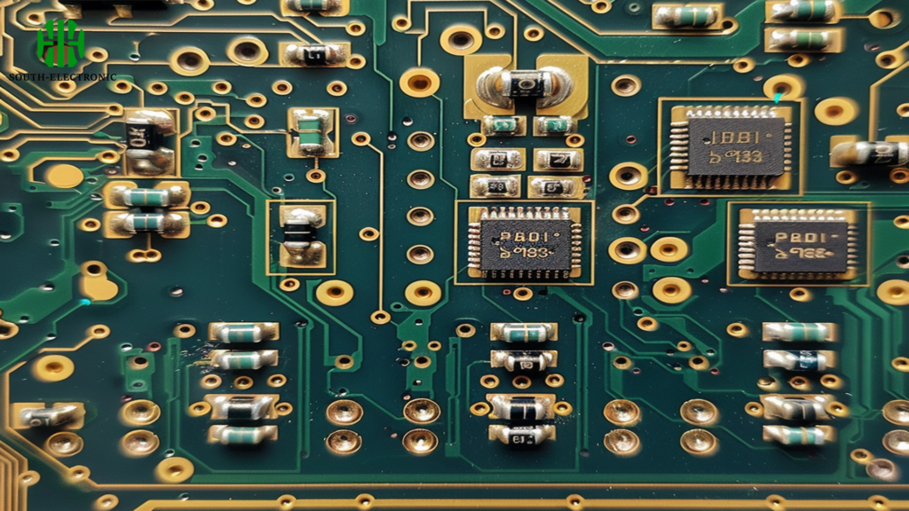
What is PCB Pad?
A PCB pad is a metal area on the surface of a printed circuit board (PCB) where component leads are soldered to create electrical connections. Pads are important for creating reliable solder joints, providing mechanical support, and making electrical connections between the conductive traces on the PCB and the components mounted on the board.
How many types of PCB pads are there?
There are three main types of PCB pads based on the components and packaging methods: through-hole pads , surface mount pads and bga pad.
Through-hole Pad
Pads for mounting through-hole components are called through-hole pads. The different parts of a via pad are often called the pad stack and include top pad, bottom pad, inner pad, drill bit, donut, pin number.
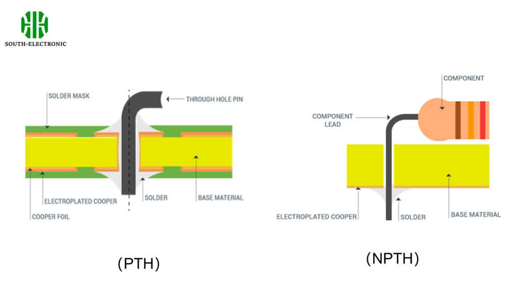
| pad shape | application |
| Plated through hole (PTH) | Hole plating is done using an electrolytic process, and the plating provides the electrical connections between the different layers of the circuit board. |
| Non-plated through hole (NPTH) | This pad is mostly used for single boards or these holes are used to mount the PCB in a case and install screws through these holes. |
Surface Mount Pad
Surface mount pads are used in surface mount technology (SMT), where components are mounted directly onto the surface of the PCB without through-holes. These pads have the following features: Pads showing the copper area. This can be a rectangle, circle, square, or other shape such as a rectangle.

| pad shape | application |
| Square pad | Printed circuit board components come in all shapes and sizes, and it’s easy to print conductors. With a hand-made PCB, you can use this pad. |
| Round pad | It is widely used in single-sided and double-sided printed boards with regularly arranged components. If the density of the board allows, the pads can be larger and will not fall off during soldering. |
| Island pad | The pad-to-pad connection becomes one. It is usually used for vertical irregular arrangements. Such pads are often used in audio recorders, for example. |
| Teardrop pad | When you connect the pads, you often use traces to keep the pads from peeling off. You disconnect the traces from the pads. You often use the pads in high-frequency circuits. |
| Polygonal pad | To differentiate pads with different outer diameters and different hole diameters to make processing and assembly easier. |
| Round pad | This pad has enough room to improve peel strength and is typically used in dual in-line packages. |
| Open pad | It is often used to make sure that the hole of the hand soldering pad is not sealed by solder after wave soldering. |
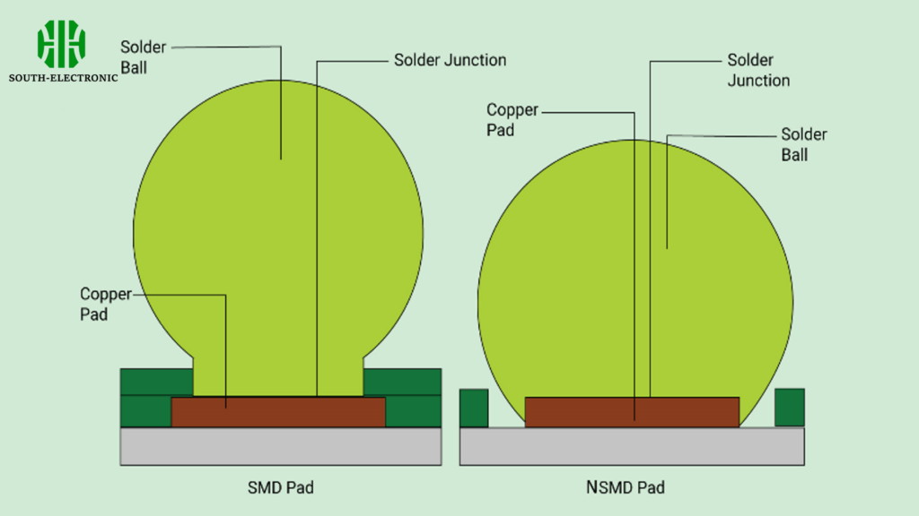
BGA Pad
When connecting BGA-type components, the correct pad design is also critical to ensure the manufacturability of the board. There are two common types of BGA pads: solder stop layer defined pads (SMD) and non-solder stop layer Defined pads (NSMD).
How to replace a pad on PCB?
Replacing a pad on a Printed Circuit Board (PCB) is a delicate process that requires precision and care, often undertaken when a pad gets lifted or damaged during soldering or desoldering components. Here’s a general guide on how to replace a pad on a PCB:
- Clean the Area: First, clean the area around the damaged pad using isopropyl alcohol to remove any flux residue or dirt.
- Remove the Damaged Pad: Carefully remove any remnants of the damaged pad using a precision knife or a dental pick. Be gentle to avoid further damage to the PCB.
- Scrape the Solder Mask: Using a precision knife, gently scrape the solder mask off the trace leading to the pad to expose the copper. This step is crucial for creating a new surface to which the new pad can adhere.
- Prepare the Replacement Pad: Cut a piece of copper foil to the size of the original pad. You can purchase copper foil that is specifically designed for PCB repairs, which often comes with an adhesive backing.
- Attach the New Pad: If the copper foil has an adhesive back, place it where the old pad was, ensuring it is properly aligned. If it doesn’t have an adhesive back, you can use a two-part epoxy glue applied both to the foil and the exposed trace. Press it down firmly and allow it to cure as per the adhesive instructions.

