

Cracked joints, misaligned parts… my PCB prototypes failed constantly back in college days. Finding the right technique fixed my electronics nightmare! Understanding reflow matters for quality circuit boards.
Reflow soldering melts solder paste using heat to attach components to PCB surfaces. This automated surface-mount process creates durable electrical connections through precise temperature management and is key for modern electronics manufacturing.
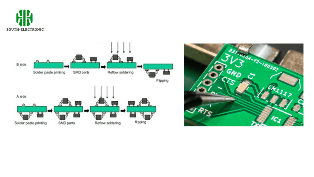
Let me unpack how this works. Reflow transforms solid solder paste into permanent bonds between components and boards. Next, we explore what happens during this critical thermal procedure.
What are the effects of PCB reflow?
My first SMT project revealed dark surprises. Overheated boards caused chip failures! Temperature errors destroy circuits quickly. The right heat creates magic while mistakes ruin entire batches.
Reflow soldering forms reliable solder joints but causes problems when temperatures stray. Effects include strong electrical connections with proper heat, while skewed solder reflow temperature risks cold joints, component damage, or board warping.
Why Effects Vary
These three factors determine outcomes:
Heat Transfer Mechanisms
| Factor | Good Result | Bad Result |
|---|---|---|
| Conduction | Even heat spread | Cold spots |
| Convection | Stable thermal transfer | Uneven heating |
| Radiation | Precise component heat | Damaged circuits |
Component Vulnerability
Some parts fail faster than others. I once fried temperature-sensitive sensors when the oven profile peaked too high. LEDs and microchips often suffer first because they absorb heat differently.
Board Materials
FR4 boards start warping after 240°C. High-temperature boards handle more stress. This structural change creates permanent bending when temperatures exceed the limit. The thicker the board, the slower the heat travels.
Poor profiles create voids in solder joints. I see bubbles under my microscope sometimes. These air gaps weaken connections and make circuits unreliable during vibration or stress tests.
Theoretical knowledge of PCB reflow path
Ever wonder why some resistors shift during heating? I tracked solder flow paths after many failed placements. Heat patterns follow physics you can predict!
The reflow path is the physical route melted solder follows during heating. Surface tension pulls solder toward hotspots. Uneven paths create misaligned parts or incomplete joints in reflow process soldering.
Following the Thermal Roadmap
Temperature Zone Behavior
| Stage | Thermal Action | Solder Response |
|---|---|---|
| Preheat | Board expands | Paste activates |
| Soak | Flux cleans surfaces | Metals pre-bond |
| Reflow | Full liquid state | Component floating |
| Cooling | Solid joint forms | Final position sets |
Component Direction Drift
Small capacitors show this clearly. They "swim" toward the hottest PCB zones. Surface tension forces are stronger on the warmer side. I place large parts last to prevent blocking the paths of smaller pieces.
Pad Geometry Effects
Round pads gather solder evenly. Rectangular pads form uneven joints at corners. Heat collects differently on angles than curves. For dense boards, avoid sharp pad edges to get consistent joint creation and prevent solder escape.
The right solder reflow temperature pulls components into alignment. Wrong profiles let them drift across pads. Understanding these movements fixes my surface-mount assembly errors every time.
What are the solutions to the reflow problem?
Trial-and-error cost me weeks fixing cold joints. Then I discovered oven calibration tools! Proper fixes save time and materials.
Key solutions include optimizing reflow soldering profiles using thermal sensors, selecting quality solder paste, and applying nitrogen atmospheres. These methods prevent common defects during the reflow process soldering.
Fixing Common Issues
Profile Correction Methods
| Problem | Tool | Action |
|---|---|---|
| Cold joints | Thermocouples | Verify zone temps |
| Component shift | Oven cameras | Track movement |
| Warping | Support pins | Hold boards flat |
Material Upgrades
Premium solder paste made the difference for me. Low-residue formulas prevent bridging on tight-pitch ICs. Pair this with nitrogen gas inside ovens to stop oxidation that causes rough joints.
Machine Adjustments
Slower cooling rates prevent thermal shock. I extend cooling time for BGAs and other dense chips. Conveyor speed changes also affect results – fast movement causes uneven temperature soaking and joint failures.
Regular maintenance matters. Cleaning oven vents weekly stopped hotspots on my home prototypes. Remember: small changes to the reflow soldering profile often fix big quality problems.
Conclusion
Optimizing reflow soldering prevents defects and strengthens PCBs. Mastering temperature control ensures reliable electronics we use daily. Always refine your thermal approach.

