
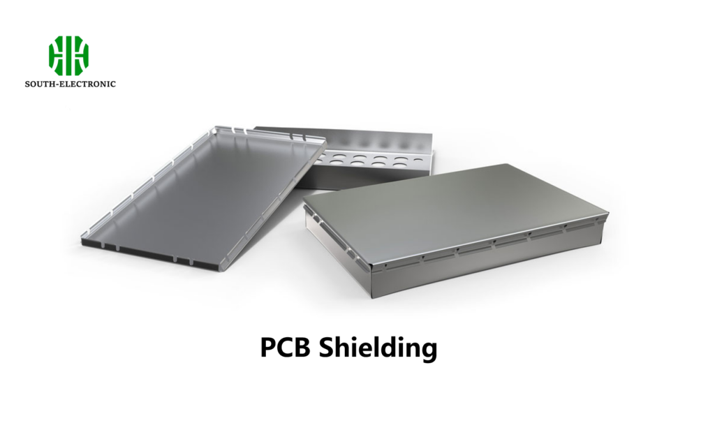
What is PCB Shielding?
PCB Shielding is the mechanical way of using conductive, magnetic, or both materials to prevent EMI in the system. These shields, connected to the ground of the PCB, effectively reduce loop antenna sizes, absorb, and/or reflect some of the radiation, ensuring the proper functioning of sensitive electronic components. From smartphones to critical medical devices, EMI has the potential to disrupt their operation, leading to malfunctions. The purpose of PCB shielding is to block, reflect, or absorb electromagnetic waves, thus preventing them from interfering with the operation of electronic components.
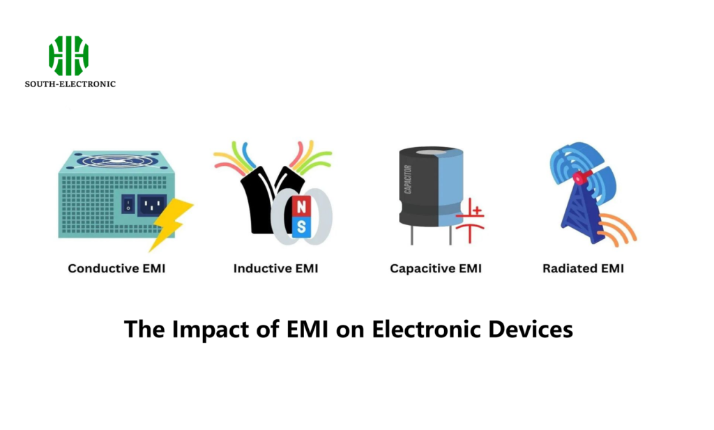
The Impact of EMI on Electronic Devices
EMI can cause a whole host of problems in electronic devices, like signal distortion, data loss, and even total device failure. For example, in medical devices, EMI can lead to incorrect readings or device malfunction, which can be a huge problem. In consumer electronics, EMI can cause all sorts of performance issues, like reduced signal strength in smartphones or Wi-Fi devices.
Real-World Examples of PCB Shielding
- Medical Devices: Shielding is critical in devices like pacemakers to ensure they function correctly in environments with high electromagnetic noise.
- Telecommunication Equipment: PCB shielding is essential in routers and modems to maintain signal integrity and prevent interference from other electronic devices.
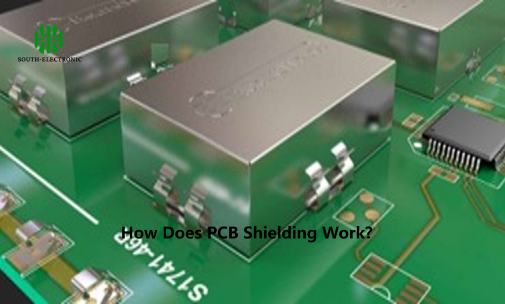
How Does PCB Shielding Work?
PCB shielding is all about creating a barrier that blocks or redirects electromagnetic waves, reducing the impact of EMI. The shielding material, usually conductive, is connected to the ground plane of the PCB, allowing it to absorb or reflect electromagnetic radiation.
- Shielding Can: A metal cover placed over components to block EMI.
- Grounding: Essential for ensuring the shield functions correctly, grounding provides a path for the absorbed EMI to dissipate.
- Shielding Materials: Common materials include copper, aluminum, and specialized conductive foams.
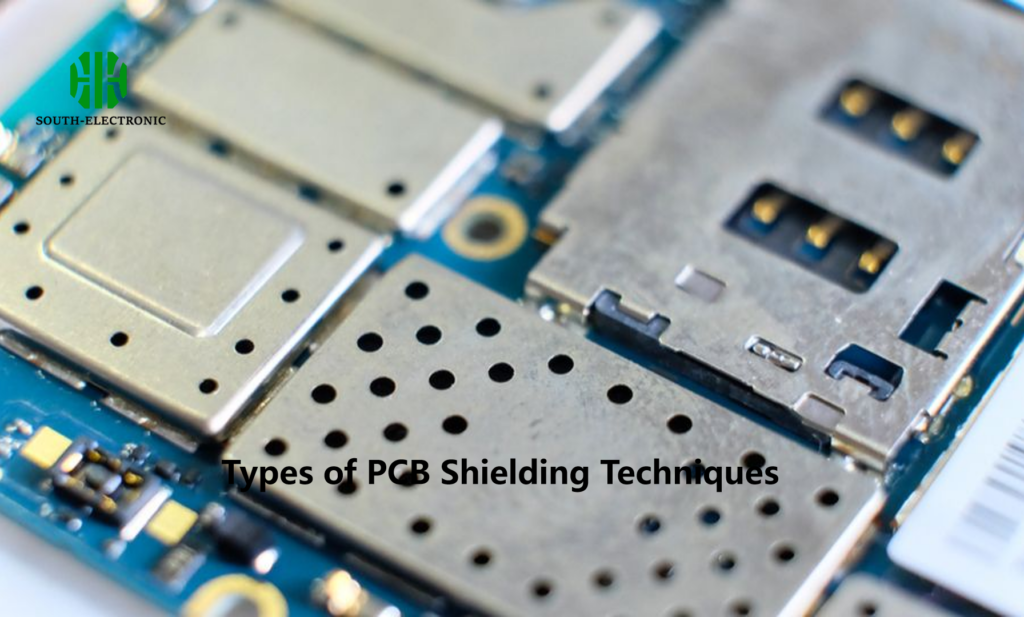
Types of PCB Shielding Techniques
There are a bunch of ways to shield PCBs. They all work a little differently, and they’re all good for different things.
1. Faraday Cage
A Faraday cage is a conductive enclosure that blocks external electric fields. In PCB design, you can do this by putting a metal box around the sensitive components and connecting it to the ground.
2. Ground Plane Shielding
A ground plane is a layer of conductive material in the PCB that’s usually connected to the ground. This layer acts as a shield for the entire board, giving it a low-impedance path to dissipate EMI.
3. EMI Shielding Gaskets
These are little conductive gaskets that you put around the edges of shielding cans or enclosures to keep EMI from leaking in or out.
Materials Used in PCB Shielding
When it comes to PCB shielding, the materials you choose are critical. They need to be conductive, lightweight, and compatible with the PCB manufacturing process.
Common Materials
| Material | Properties | Common Uses |
|---|---|---|
| Copper | High conductivity, excellent for EMI shielding, easily integrated into PCB designs. | Used in high-frequency applications. |
| Aluminum | Lightweight, cost-effective, good conductivity, but less effective at high frequencies. | Used in consumer electronics, lightweight devices. |
| Conductive Foam | Flexible, can be molded into complex shapes, provides cushioning as well as shielding. | Used in mobile devices, where flexibility is needed. |
The choice of material depends on several factors, including the operating frequency of the device, the size constraints of the PCB, and the cost considerations. For high-frequency applications, copper is often preferred due to its superior shielding properties. However, for low-cost consumer electronics, aluminum might be more suitable.

Challenges in PCB Shielding
While PCB shielding is essential, it also presents several challenges, particularly in the design and manufacturing stages.
1. Space Constraints
As devices become smaller, finding space on the PCB for effective shielding can be difficult. Designers must balance the need for shielding with the limited real estate available on the board.
2. Cost
Shielding materials and techniques can add significant cost to the PCB. This is particularly challenging in consumer electronics, where cost is a critical factor.
3. Design Complexity
Incorporating shielding into a PCB design can complicate the manufacturing process. Designers need to carefully plan the placement of shielding components to avoid interference with other parts of the board.
In today’s complex electronic environment, PCB shielding is essential for ensuring the reliable operation of electronic devices. By blocking, reflecting, or absorbing electromagnetic interference, PCB shielding protects sensitive components and prevents malfunctions. Whether in telecommunications, healthcare, or automotive applications, effective PCB shielding is a critical aspect of modern electronics design.

