
Do EMI issues plague your PCB designs? Signals drowning in interference nightmares? PCB via stitching solves this by creating multiple conductive pathways. I use it like digital armor against noise disasters.
PCB via stitching strategically places clusters of tiny conductive holes (vias) between copper layers. This creates parallel return paths that boost current flow while suppressing electromagnetic interference. It’s your board’s essential noise-cancelling system.
This technique transforms circuit performance completely. Now see exactly how it blocks interference, shields your signals, and avoids production pitfalls.
How does via stitching act as your PCB’s shield against EMI?
Noisy circuits crippling your device reliability? EMI radiation escapes easily without proper containment. Stitching vias creates an invisible electromagnetic barrier.
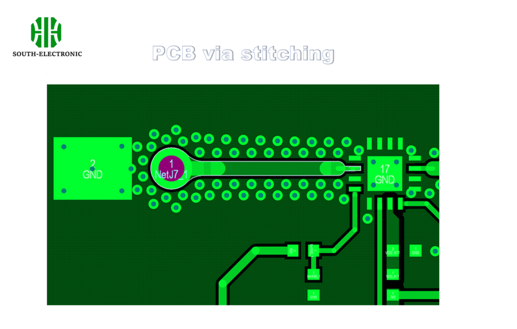
Via fences around sensitive components form localized Faraday cages. These grouped vias confine disruptive fields like a mesh barrier. Current loops naturally take the stitching path instead of radiating outward.
Breaking Down EMI Mitigation
Three mechanisms combine in via stitching defense:
| Defense Layer | How It Works |
|---|---|
| Return Path | Provides numerous parallel return routes for edge currents |
| Field Containment | Short gaps between vias trap electromagnetic field energy |
| Ground Coupling | Direct anchor to ground planes lowers overall system impedance |
I see vias as miniature lightning rods. They sink destructive energy into ground before interference spreads. High-density placement creates critical surface coverage. Think of stitching patterns as creating electromagnetic moats around circuit zones. The spacing between vias determines containment strength – closer gaps achieve complete blocking. Shorter vertical connections also lower inductance, especially vital above 1GHz. One project reduced EMI by 18dB simply by doubling stitch density around oscillators.
Can via stitching rescue high-speed traces for signal integrity?
Signal distortions killing data transmission? High-frequency designs suffer from reflections without controlled impedance. Via stitching stabilizes return currents critical for clean waveforms.
Parallel stitch rows beside traces maintain consistent reference planes. This prevents impedance discontinuities during layer transitions. I avoid signal path stutters through uniform current paths.
Signal Rescue Tactics
Speed demands precise stitching management:
| Challenge | Stitching Solution |
|---|---|
| Return Path Gaps | Stitching bridges reference plane seams with continuous current paths |
| Skin Effect | Multiple vias distribute high-frequency surface currents equally |
| Crosstalk | Via barriers absorb EM field spillage between adjacent traces |
For multi-gigabit signals, signal stitches must mirror each bend and turn. I place pairs within 0.5mm of critical traces. Each ground stitch sinks electromagnetic interference before it corrupts adjacent signals. Power integrity gains from stitching too – a dense grid lowers impedance. Remember to match stitch density to frequency demands. More vias equal better noise immunity but consider manufacturability limits.
How does over-stitching kill your PCB yield?
Drilled PCB looking like swiss cheese? Excessive vias increase fabrication risks. Your design faces potential failures with uncontrolled via density.
Packed vias crack under thermal stress during assembly. Stitch clusters cause localized warping during reflow. I’ve seen solder wick into unused vias causing opens in high-yield boards.
The Fracture Point
Balance protection against production failures:
| Fabrication Risk | Root Cause |
|---|---|
| Pad Cratering | Dense vias weaken copper adhesion during thermal cycling |
| Drill Wander | Tiny drill bits deflect in clustered patterns affecting hole alignment |
| Resin Starvation | Close holes reduce epoxy flow creating air pockets in laminates |
Manufacturers flag designs exceeding via-per-square-inch limits. My rule: place stitches every other pad in RF zones, sparingly elsewhere. Thermal analysis shows how via clusters act as heat bridges – uneven expansion causes fractures. Use stitching strategically near problem parts only. Blind vias reduce through-hole damage but increase cost. Measure EMI reduction against yield impact – sometimes 30% fewer vias save 60% board failures.
Conclusion
PCB via stitching transforms noise suppression and signal integrity when implemented correctly. Balance EMI protection against manufacturing realities for optimal results.

