
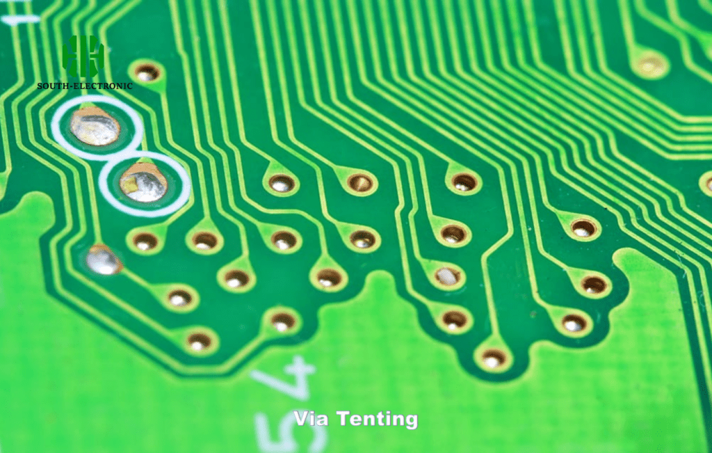
Imagine solder creeping into your vias during assembly. This contamination could create short circuits or weaken connections. Tented vias solve this by coating via openings with soldermask, protecting your PCB from soldering mishaps.
PCB via tenting is the process of covering via holes with soldermask to prevent solder intrusion and contamination. This method improves reliability while offering environmental protection for your circuit board during manufacturing and operation.
Choosing between tented and untented vias affects manufacturing costs, signal performance, and durability. Let’s explore how this subtle design decision impacts your PCB’s functionality across different scenarios.
Tented Vias vs. Untented Vias: Which Is Better for Your PCB Design?
Trapped air in sealed vias expands during thermal spikes, risking layer separation. Untented vias avoid this issue but expose copper to oxidation. Your decision depends on operating conditions and performance priorities.
Tented vias suit harsh environments requiring pollution protection, while untented vias allow airflow for thermal management. Choose tenting for consumer electronics needing reliability; leave vias open for high-power industrial boards requiring heat dissipation.
Key Design Considerations
Three factors determine via treatment suitability:
| Criteria | Tented Vias | Untented Vias |
|---|---|---|
| Moisture Resistance | Excellent | Poor |
| Thermal Cycling | Risk of pressure buildup | No pressure issues |
| Solder Mask Alignment | Critical | Not applicable |
High-humidity applications like automotive electronics benefit from tented vias’ sealed protection. However, boards experiencing rapid temperature changes (e.g., LED streetlights) risk delamination due to trapped gas expansion. Untented vias work better here but require immersion silver or gold plating to prevent copper degradation.
Does Via Tenting Improve Signal Integrity in High-Speed Circuits?
Reflections occur when impedance mismatches plague your GHz-range signals. Tented vias alter capacitance, potentially disrupting carefully tuned transmission lines.
Via tenting slightly increases parasitic capacitance due to soldermask dielectric properties. For signals below 5 GHz, this effect is negligible. However, millimeter-wave designs above 24 GHz may require untented vias or specialized materials.
High-Frequency Tradeoffs
Three impacts of via treatment on RF performance:
| Frequency Range | Tented Via Effect | Mitigation Strategy |
|---|---|---|
| 10 GHz | Significant resonance risk | Use via-in-pad or untented |
In a recent router PCB redesign, tenting 2.4 GHz antenna feed vias caused 0.3 dB loss increase. Removing solder mask from those specific vias restored performance without compromising overall protection. Always simulate critical signal paths with your stack-up’s exact soldermask Dk value.
How to Implement Via Tenting: Design Rules and Manufacturing Tips
A designer once tented 0.2 mm vias but forgot mask clearance rules. The result? Uncovered vias caused 12% board failures. Proper DFM prevents such costly errors.
Always specify 0.05 mm soldermask overlap on via pads. Maintain 0.1 mm clearance between mask openings and adjacent traces. Use “tenting” in your fab notes and verify with Gerber viewer inspections.
Manufacturing Checklist
Five essential rules for successful via tenting:
| Rule # | Parameter | Value | Reason |
|---|---|---|---|
| 1 | Minimum via diameter | 0.3 mm | Ensures proper mask coverage |
| 2 | Soldermask expansion | -0.05 mm | Prevents mask over-removal |
| 3 | Via-to-trace distance | 2x mask thickness | Avoids mask bridging defects |
| 4 | Annular ring width | 0.15 mm | Provides anchoring for mask |
| 5 | Max aspect ratio | 8:1 | Prevents incomplete tenting |
When prototyping, request tenting test coupons from your manufacturer. These verify mask adhesion strength and coverage consistency across different via sizes. For HDI designs with microvias, confirm your fabricator’s laser-drilling compatibility with tented openings.
Conclusion
Via tenting balances protection and performance. Match via treatment to environmental needs and signal speeds, adhere to DFM rules, and validate with prototyping for reliable PCB operation across applications.


