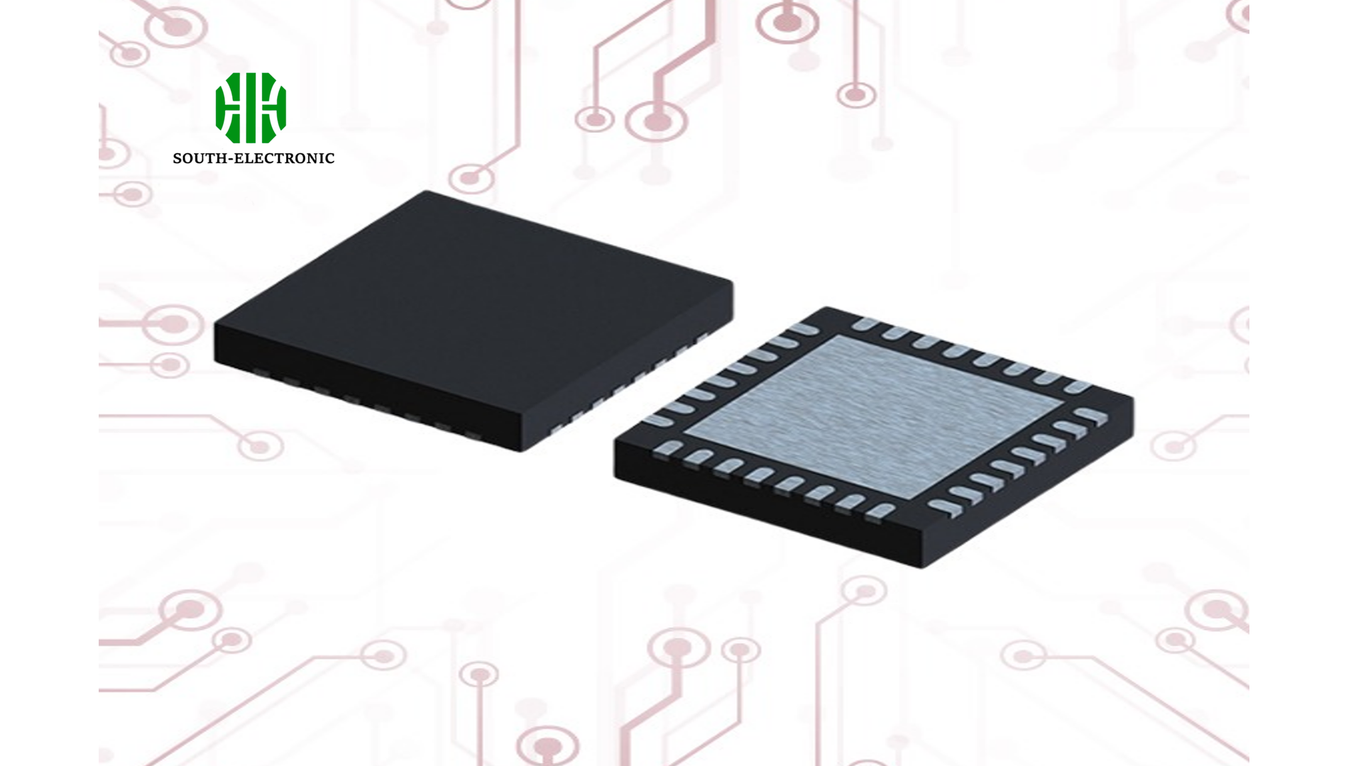
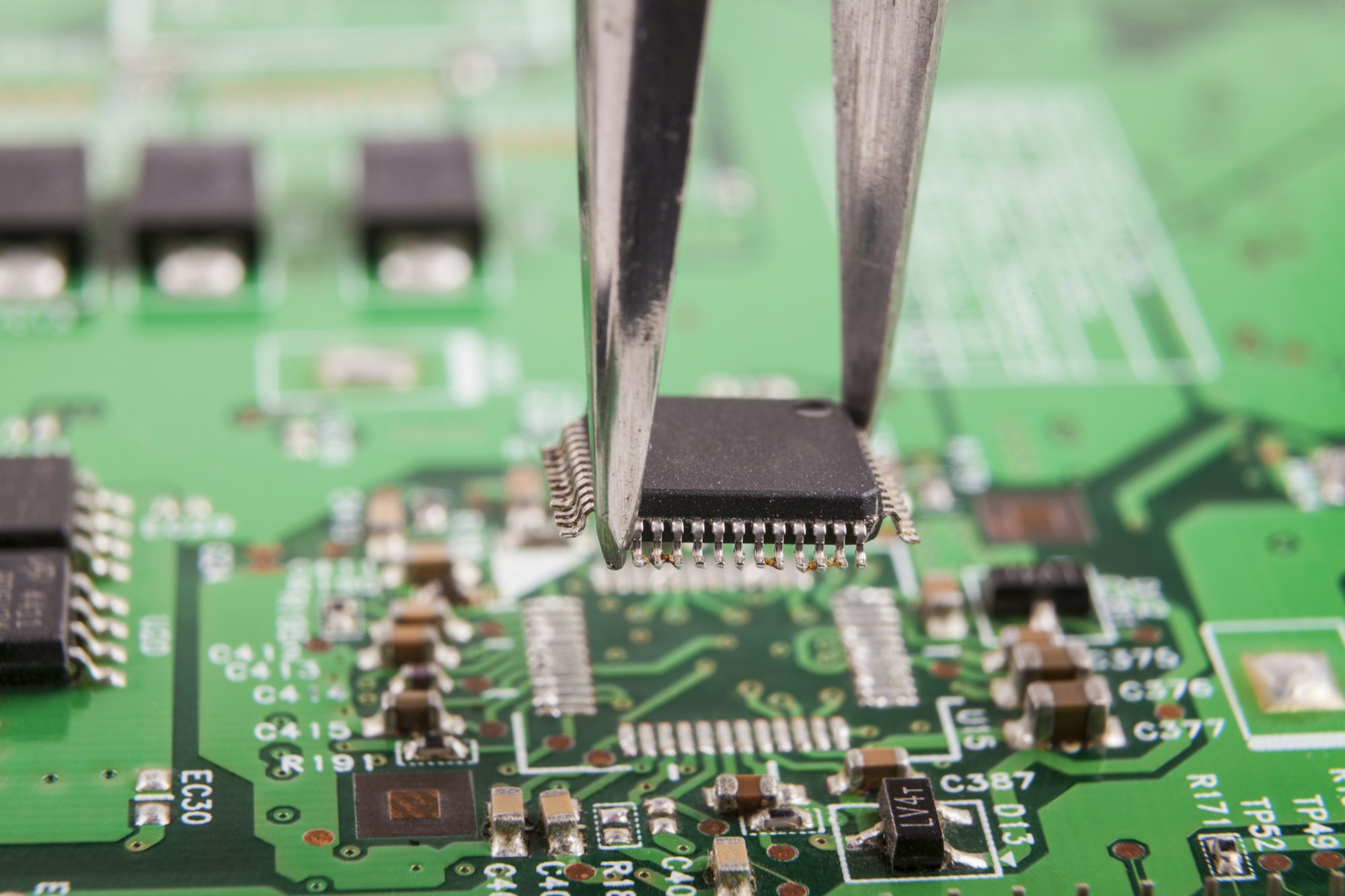
What is the QFN Package?
The QFN(Quad Flat No-lead) package is a surface-mount technology designed for ICs. It has a leadframe design without traditional protruding leads, which provides a compact and efficient solution for connecting ICs to a PCB. The QFN package is widely used in applications where size, weight, and thermal performance are critical factors.
Here’s a quick breakdown of its key features:
| Feature | Description |
|---|---|
| Leadless Design | The absence of external leads makes QFN packages smaller and lighter. |
| Thermal Pad | QFNs often have an exposed thermal pad, providing excellent heat dissipation. |
| Low Profile | QFNs are designed to have a low vertical profile, making them suitable for high-density applications. |
| Small Footprint | Their compact size makes them ideal for applications with space constraints. |
What is the Quad Flat No-lead Package Used For?
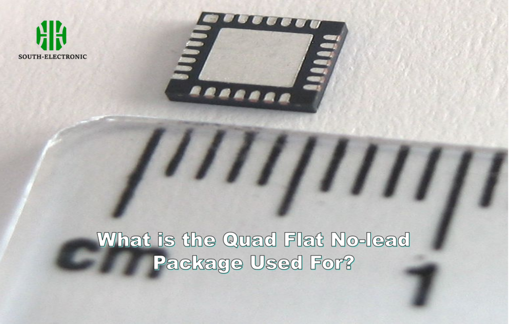
The primary function of a QFN package is to physically and electrically connect integrated circuits to a PCB using surface-mount technology (SMT). Thanks to its small size, low cost, and effective heat dissipation, the QFN package is used in various industries, including:
- Consumer Electronics: Smartphones, tablets, and wearable devices often use QFN packages to optimize space and performance.
- Automotive: QFN is ideal for automotive electronics, where heat dissipation and reliability are key.
- Telecommunications: Wireless and networking equipment benefit from the compact nature of QFN packages.
- Industrial Applications: Robotics and automation equipment rely on QFN for its performance in harsh environments.
Types of QFN Packages
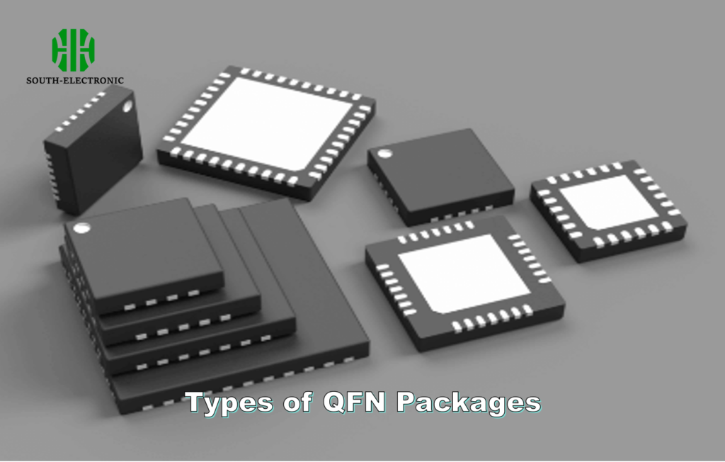
There are several types of QFN packages, each designed to suit different applications. Let’s break down the most common variations:
1. Single-row QFN
In this configuration, the contacts (pads) are located around the perimeter of the package, making it ideal for simple circuits that don’t require high-density interconnections.
2. Dual-row QFN
This type features an additional row of pads inside the perimeter, providing more contact points. Dual-row QFN is useful for applications that need more connections while still maintaining a small footprint.
| QFN Type | Description | Applications |
|---|---|---|
| Single-row | Pads are located only on the perimeter. | Low to moderate connection density. |
| Dual-row | Additional pads inside the perimeter. | High connection density in compact areas. |
3. Air-cavity QFN
This variant includes a cavity between the die and the package lid to prevent moisture buildup and improve performance at higher frequencies, making it ideal for RF applications.
Advantages and Disadvantages of QFN Packages
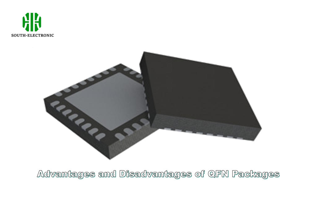
Advantages:
- Compact Size: The leadless design reduces the package’s overall size, making it perfect for high-density boards.
- Improved Thermal Performance: QFNs often come with an exposed pad on the underside, which enhances heat dissipation.
- Low Cost: The simpler construction and smaller size make QFN packages more cost-effective than other packaging types.
- Better Electrical Performance: The shorter lead length reduces parasitic inductance, improving signal integrity.
Disadvantages:
- Oxidation Issues: Since QFN packages don’t have leads, they are more prone to oxidation, which can affect solderability.
- Soldering Challenges: The lack of leads also creates challenges when soldering, as clearance issues can arise between the reflow pads and soldering tools.
- Floatation Problems: QFN packages can “float” during reflow soldering, which can result in uneven connections.
QFN Package Sizes and Footprint
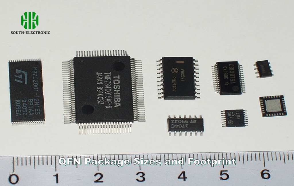
QFN packages come in a variety of sizes to accommodate different applications. These sizes are typically measured by the number of contact pads and the overall dimensions of the package.
For instance:
- 4×4 mm QFN: Small, ideal for mobile devices.
- 7×7 mm QFN: Suitable for more complex circuits requiring more pads.
- 9×9 mm QFN: Often used in power management ICs where heat dissipation is critical.
Below is a table showing common QFN sizes:
| Package Size (mm) | Number of Pins | Applications |
|---|---|---|
| 4×4 | 16 | Mobile devices, sensors |
| 7×7 | 32 | Communication ICs |
| 9×9 | 48 | Power management, automotive ICs |
QFN vs QFP Package: Which One Should You Choose?
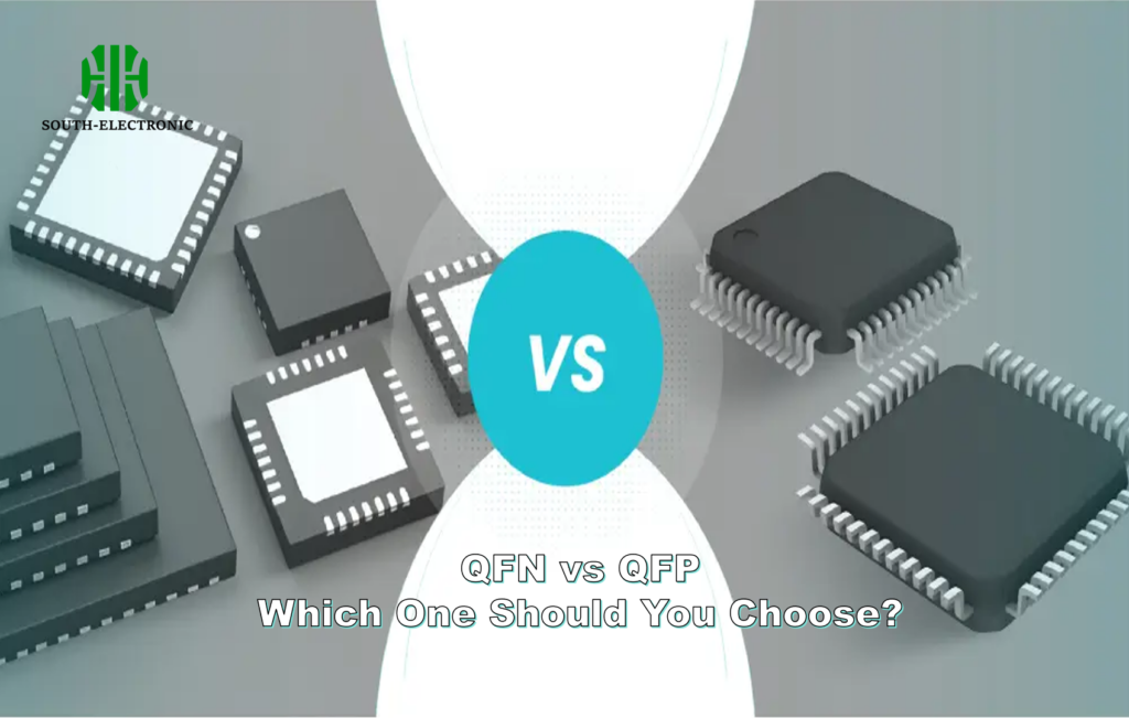
A common question in the electronics industry is how QFN compares to other packaging types like QFP (Quad Flat Package). Here’s a quick comparison:
| QFN (Quad Flat No-lead) | QFP (Quad Flat Package) |
|---|---|
| No external leads | Has extended leads (pins) |
| More compact and lower profile | Slightly larger due to the external leads |
| Better thermal performance | Moderate thermal dissipation |
| More challenging to solder | Easier to solder with visible pins |
When choosing between QFN and QFP, engineers should consider the application’s thermal requirements, space constraints, and ease of manufacturing.
In conclusion, the QFN package is a versatile, efficient, and cost-effective solution for connecting integrated circuits to PCBs. Its leadless design, compact size, and improved thermal performance make it an excellent choice for a wide range of applications, from consumer electronics to automotive systems. However, engineers must also be aware of the potential challenges, such as oxidation and soldering difficulties, and weigh these against the advantages.

