
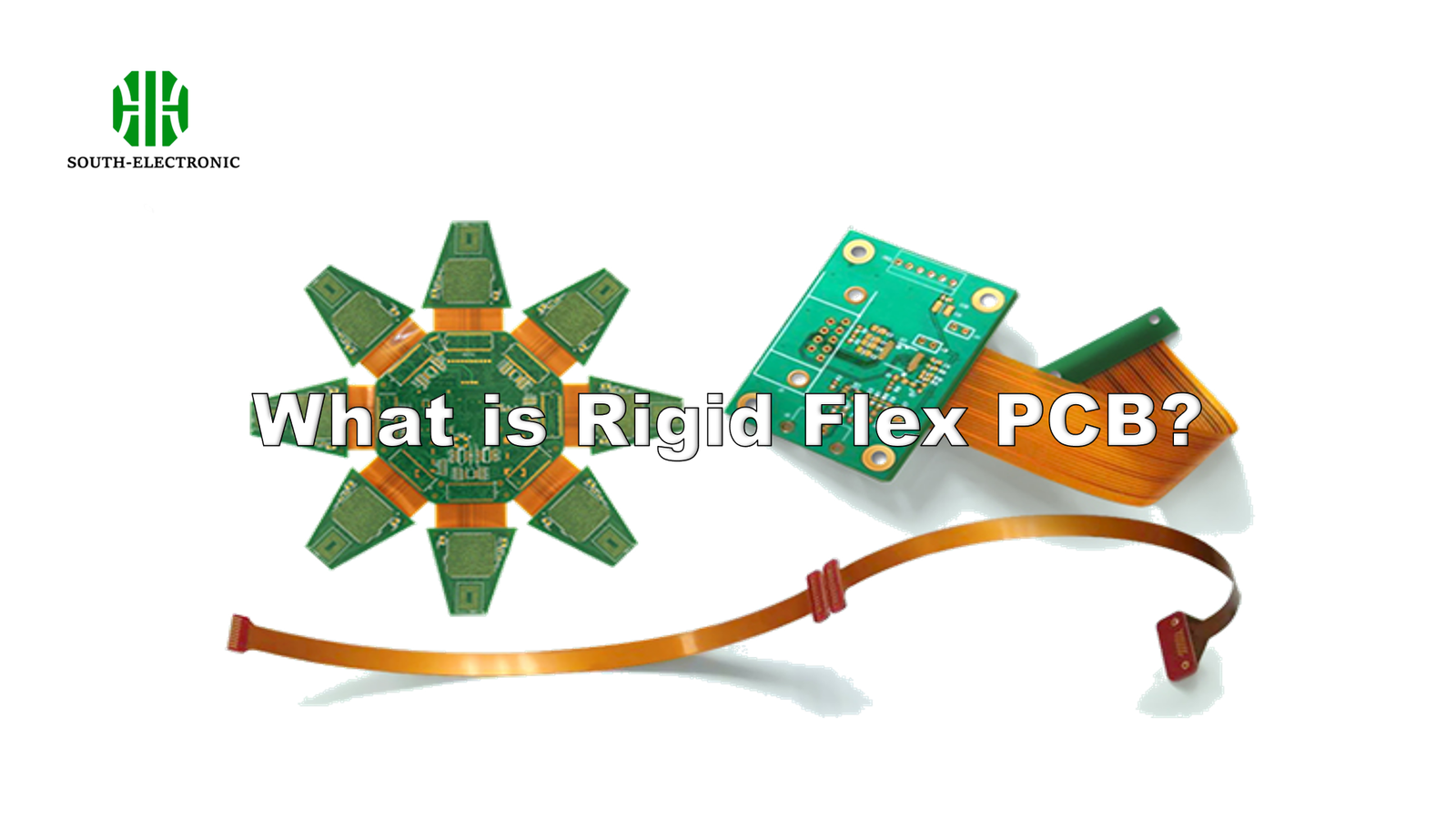
Have you ever struggled with circuit boards that crack under pressure or force engineers to make space-wasting design compromises? Traditional PCBs can’t bend – until now.
Rigid-flex PCBs[^1] combine rigid and flexible circuit materials into a single 3D structure, eliminating connectors while improving reliability in bend-critical applications like medical implants and aircraft systems. These hybrid boards achieve 50-70% weight reduction compared to conventional PCB assemblies according to IPC standards.
Let’s dissect why major tech companies are converting to rigid-flex solutions and how to avoid implementation pitfalls that could derail your next hardware project.
Key Advantages of Rigid-Flex PCB?
Why would engineers choose complex rigid-flex designs over conventional boards? The answer lies in three game-changing benefits.
Rigid-flex PCBs reduce connector failure points[^2] by 83% while enabling 360-degree component placement in 3D space, making them essential for foldable electronics and mission-critical aerospace systems. Military studies show 40% improvement in vibration resistance[^3] compared to traditional PCB assemblies.
Structural Advantages Unveiled
Modern rigid-flex designs solve four critical engineering challenges:
| Challenge | Rigid PCB | Flex PCB | Rigid-Flex PCB |
|---|---|---|---|
| 3D Layout | Limited | Partial | Full 360° |
| Vibration | 6G Limit | 8G | 12G Tolerance |
| Weight | 100% | 70% | 50-60% |
| Connectors | 15-30 | 5-10 | 0-3 |
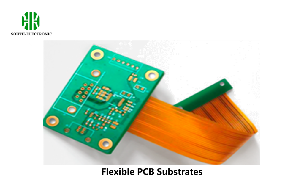
From smartwatch motors to satellite components, this hybrid approach enables thinner profiles while maintaining circuit integrity under mechanical stress. The secret lies in polyimide flex layers[^4] bonded to FR4 rigid sections through patented lamination processes.
How Rigid-Flex PCBs Work?
What physical principles enable circuits to bend without breaking? It’s all about strategic material engineering.
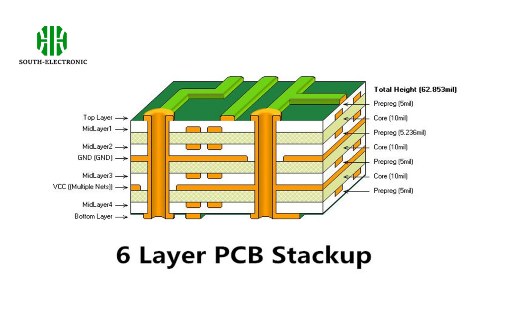
Rigid-flex boards alternate stiffener layers with dynamic flex zones using controlled impedance traces[^5], achieving over 200,000 bend cycles in wearables while maintaining signal integrity. IPC-6013D standards specify 8-layer minimum constructions for high-reliability applications.
)
The Flex-Rigid Matrix Explained
Five elements define successful rigid-flex implementation:
-
- Minimum 10X material thickness
- Static vs dynamic bending requirements
-
Adhesive Selection[^7] Type Temp Range Flexibility Acrylic -55°C-125°C Medium Epoxy -40°C-110°C Low Silicone -100°C-200°C High -
Stiffener Placement
Strategic FR4/Polyimide transitions prevent solder joint fractures -
Conformal Coatings
Protect dynamic flex areas from moisture/environmental damage -
Testing Protocols
85/85 TH testing[^8] (85°C/85% RH) validates automotive-grade reliability
Medical device manufacturers report 99.98% reliability rates when following these design protocols in pacemaker implementations.
Common Challenges in Rigid-Flex PCB Manufacturing?
Why do 68% of first-time rigid-flex projects miss deadlines? Three hidden hurdles trip up even experienced teams.
Material shrinkage during lamination causes up to 0.3% dimensional variance, requiring precise thermal compensation algorithms and 5-axis laser drills for microvia alignment. NASA JPL reports 22% yield improvement using vacuum lamination presses.
Manufacturing Minefield Breakdown
Critical phase-specific challenges include:
Design Phase
- Mixed Dk values causing impedance mismatches
- Coefficient of thermal expansion (CTE) conflicts[^9]
Prototyping
- Average 4-6 spin cycles for bend radius validation
- $12,000-25,000 tooling costs for complex shapes
Mass Production
- 3X longer etching times for polyimide vs FR4
- Special handling to prevent flex layer delamination
Leading manufacturers like TT Electronics use AI-driven shrinkage prediction models[^10] to achieve ±0.05mm layer alignment – critical for 16+ layer military/aerospace designs.
Rigid vs. Flexible vs. Rigid-Flex: Which PCB is Right for Your Project?
Choosing the wrong PCB type can increase BOM costs by 300%[^11] – how to decide?
Select rigid boards for cost-sensitive 2D layouts, pure flex for dynamic bending needs under 5mm radius, and rigid-flex for 3D high-reliability systems requiring <0.3% failure rates over 100k+ cycles. Automotive ADAS systems show 40% cost savings using rigid-flex versus connector-heavy alternatives.
)
Decision Framework for Engineers
Use this scoring matrix to optimize selection:
| Criterion | Rigid (1-5) | Flex (1-5) | Rigid-Flex (1-5) |
|---|---|---|---|
| 3D Capability[^12] | 1 | 3 | 5 |
| High-Speed Signals | 5 | 2 | 4 |
| Vibration Resistance | 2 | 4 | 5 |
| Upfront Cost | 5 | 3 | 2 |
| Assembly Complexity | 5 | 2 | 3 |
| Weight Efficiency | 2 | 4 | 5 |
Consumer electronics typically choose rigid-flex when product thickness must stay under 8mm with bending requirements, while industrial controls often opt for cost-effective rigid boards.
Conclusion
Rigid-flex PCBs solve critical space and reliability challenges in modern electronics, but require careful implementation of material science and thermal management[^13] principles for successful deployment.
[^1]: Explore this link to understand how Rigid-flex PCBs can revolutionize your designs with their unique advantages and applications.
[^2]: Learn about the significant reduction in connector failure points with Rigid-flex PCBs and how it enhances reliability in critical applications.
[^3]: Discover the impressive vibration resistance of Rigid-flex PCBs and why they are preferred in demanding environments like aerospace.
[^4]: Learn about polyimide flex layers and their crucial role in enhancing the performance and durability of electronic circuits.
[^5]: Discover how controlled impedance traces improve signal integrity in PCBs, essential for high-performance electronic applications.
[^6]: Understanding Bend Radius Control is crucial for ensuring the longevity and reliability of rigid-flex PCBs. Explore this link for in-depth insights.
[^7]: Choosing the right adhesive is vital for performance and durability in rigid-flex applications. This resource will guide you through the selection process.
[^8]: 85/85 TH testing is essential for validating the reliability of PCBs in harsh environments. Discover more about its significance and application here.
[^9]: Understanding CTE conflicts is crucial for ensuring product reliability and performance in manufacturing processes.
[^10]: Explore how AI models enhance precision in manufacturing, leading to better quality and reduced costs.
[^11]: Learn about the significant impact of PCB selection on overall project costs and efficiency in manufacturing.
[^12]: Discover why 3D Capability is essential in PCB design and how it can optimize your engineering projects.
[^13]: Learn about the crucial role of material science and thermal management in PCB design for improved performance and reliability.

