

Have you ever opened an electronics kit and felt overwhelmed? Confusing component names made assembly terrifying. That frustration vanishes when clear markings guide you instantly.
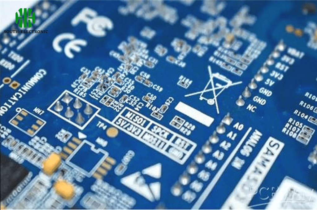
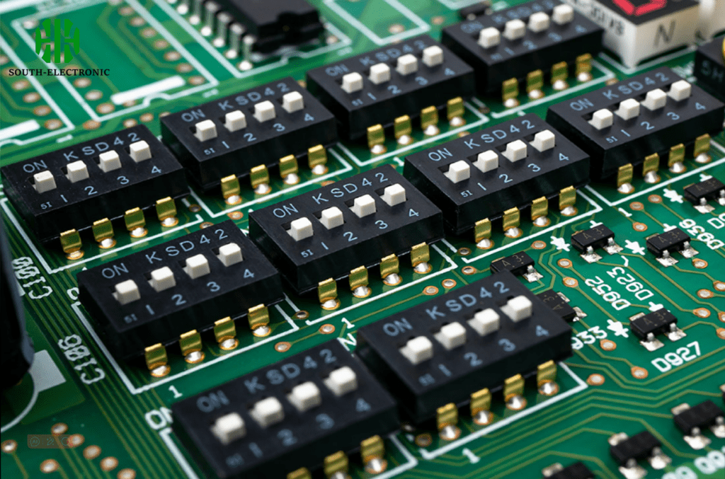
Silkscreen on a PCB refers to the topmost printed layer using white ink to add text, symbols, and markings. This essential layer helps identify components during assembly and testing, ensuring correct board construction.
Now that we understand its core purpose, let’s explore different aspects of silkscreen technology. This knowledge simplifies troubleshooting and design choices.
Types of PCB Silkscreen[^1]?
Ever chosen the wrong printing method? Poor resolution silkscreen caused mislabeled resistors on my first prototype. Fixing assembly errors wasted precious development days.
Three primary silkscreen methods exist: manual screen printing[^2], Liquid Photo Imaging (LPI), and Direct Legend Printing. Each suits different design complexities and cost requirements.
Comparing Silkscreen Application Methods
Various techniques accommodate diverse manufacturing needs. Understanding differences prevents design flaws.
Resolution Capabilities
| Method | Line Width | Ideal Use Case |
|---|---|---|
| Manual Printing | ≥0.007 inches | Large components |
| LPI | ≥0.004 inches | High-density boards |
| Direct Printing | ≥0.003 inches | Fine-pitch IC markings |
Manufacturing Factors
LPI uses photolithography for precision. A photosensitive liquid hardens under UV light through a film mask. Unexposed areas wash away, leaving crisp markings. This method handles complex layouts well but increases costs. Manual screen printing employs polyester mesh stencils. Squeegees force ink through open areas. It’s economical for larger text but struggles with tiny fonts. Direct Printing utilizes inkjet technology. Print heads deposit ink digitally without masks. Setup costs drop for small batches, and font sizes adjust freely. However, ink adhesion varies across board materials. Surface roughness affects readability. Choosing wrongly risks blurred component indicators during reflow cycles.
What is Silkscreen in Art?
Saw a vibrant band poster but couldn’t reproduce the texture? My initial prints came out muddy. Traditional methods failed to capture intricate gradients effectively.
Silkscreen in art, or printmaking screen printing, forces ink through mesh stencils onto surfaces. Artists create layered, multi-color designs on fabrics, paper, and unconventional mediums like wood.
From Canvas to Circuit Board
Though sharing principles, artistic and PCB silkscreen printing differ fundamentally in execution.
Screen Printing Process Comparison
| Aspect | Artistic Screen Printing | PCB Silkscreen |
|---|---|---|
| Color Layers | Multiple separations | Single (typically white) |
| Substrates | Textiles/paper/canvas | Fiberglass/Solder Mask |
| Precision | Visual alignment | Microscopic calibration |
Creative Technical Workflow
Art screen printing starts with emulsion-coated screens. Artists expose designs using sunlight or UV units. Each color needs a separate screen. Hand pressing forces ink through open mesh areas. Proper registration prevents blurring. PCB methods prioritize longevity under heat. Industrial inks withstand soldering temperatures. Artists explore water-based pigments for ecological pieces. Thickener additives adjust viscosity. Pressure consistency ensures even coverage. Both fields require meticulous stencil preparation and drying control. While electronics focus on function, artistic screen printing enables tactile textures impossible digitally. Each layer builds dimensional richness through overlapping colors. This manual process remains popular despite digital alternatives.
How is PCB Silkscreen Applied?
Ever had silkscreen smear during assembly? My client encountered this with budget boards. Their labels disappeared during wave soldering, complicating repairs.
PCB silkscreen application[^3] follows sequential chemical steps. Ink adheres to solder mask via cleaning, printing, and thermal curing. Precise alignment prevents obscured test points.
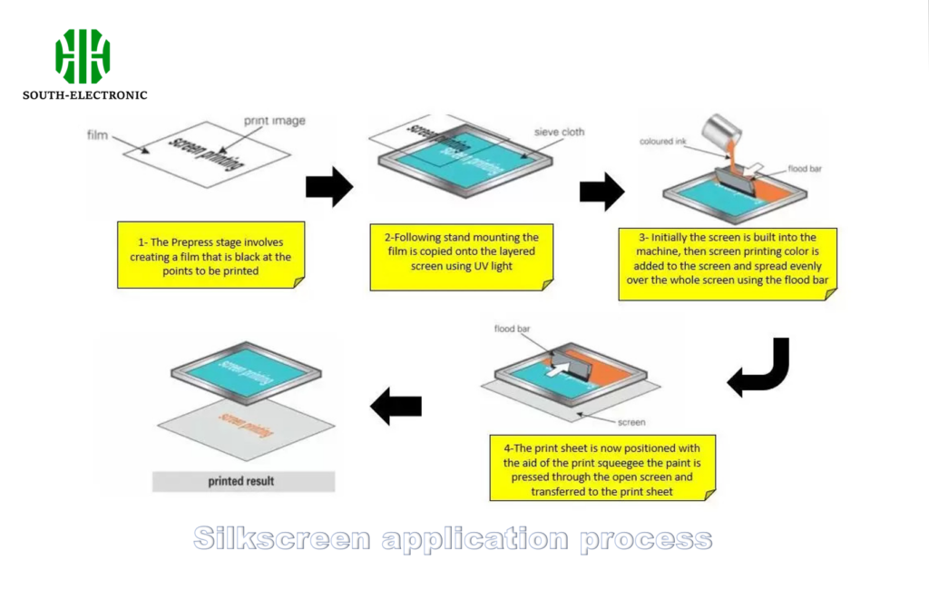
Step-by-Step Manufacturing Journey
Every production phase demands environmental control to guarantee legibility under stress conditions.
Critical Application Parameters
| Stage | Key Variables | Failure Risks |
|---|---|---|
| Surface Prep | Cleanroom particle count | Ink peeling |
| Printing | Squeegee angle/speed | Incomplete character fill |
| Curing | Temperature/duration | Charring or flaking |
Process Flow Deep Dive
Boards first undergo solvent cleaning. Oil residues impede ink bonding. Technicians load cleaned PCBs into jig frames. LPI application involves roller-coating epoxy-based ink. Liquid level sensors maintain uniform thickness. Pre-baking removes solvents at 75°C. Aligned photomasks hit UV exposure units. Light hardens protected sections. Developers spray alkaline solutions to dissolve unaffected zones. Final curing at 140°C solidifies patterns. Manual printing skips chemical steps. Operators align mesh screens visually. Ink application requires steady pressure. Direct printing employs cartridge dispensers. Software calibrates nozzle paths. IR lamps dry deposits instantly. Post-process inspections magnify markings 40x. Defective boards undergo rework or rejection. Proper humidity control prevents viscosity shifts throughout.
Conclusion
PCB silkscreen provides vital board markings for identification and assembly. Selecting the appropriate printing method ensures lasting readability across production.
[^1]: Understanding PCB Silkscreen is crucial for anyone involved in electronics design and assembly, ensuring accurate component identification and assembly.
[^2]: Learning about screen printing methods can inspire creativity in both art and electronics, showcasing the versatility of this technique across fields.
[^3]: Learn about the critical steps in PCB silkscreen application to ensure quality and durability in electronic components.

