

Ever struggle to find components on a crowded PCB? Misplaced parts cost time and money. Imagine assembly errors causing product failures. Silkscreen solves these frustrations with clear labeling.
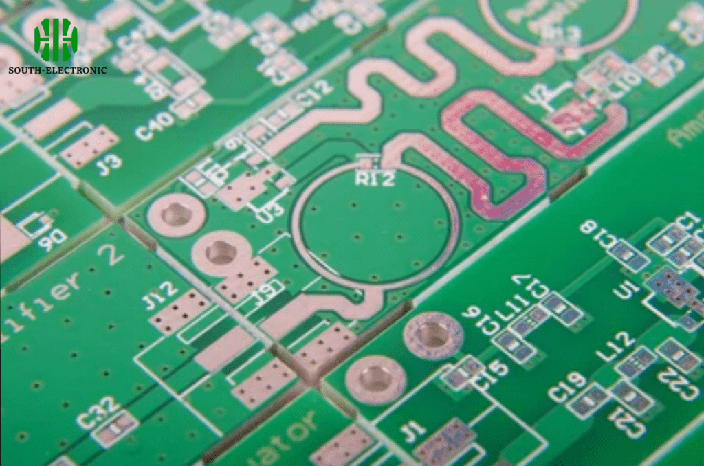
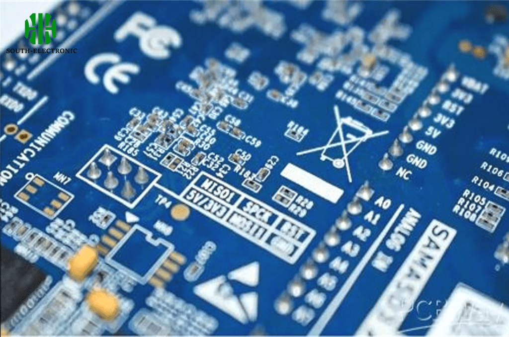
Silkscreen printing PCB applies non-conductive epoxy ink onto boards. It labels components like resistors and capacitors directly. This white lettering helps assembly and troubleshooting. Technicians quickly see where each part belongs. Errors drop sharply during manufacturing and repair.
Knowing silkscreen basics is just the start. Next we’ll explore practical types and money-saving designers use every day.
What are the common types of PCB silkscreen?
Frustrated with blurry or unreadable component labels? Inaccurate markings ruin boards. I recommend choosing the right printing method for clarity.
Three main methods handle PCB silkscreen printing. Manual remains best for simple DIY projects. LPI suits dense boards needing precision. Direct printing offers speed for prototypes.
Understanding Your Silkscreen Options
Not all silkscreen methods work equally well. Each suits specific needs and budgets. See the key differences here:
| Method | Resolution | Durability | Best For |
|---|---|---|---|
| Manual screen printing | 0.3mm | Medium | Large text, hobby PCBs |
| Liquid Photo Imaging (LPI) | 0.1mm | High | Complex layouts |
| Direct legend printing | 0.05mm | Medium | Fast prototypes |
Manual screen printing uses physical stencils. You squeegee ink through mesh patterns. This works for basic silkscreen PCB jobs at home or factories. LPI applies liquid photoimageable epoxy instead. UV light hardens precise traces. Electronics makers choose LPI for tiny symbols and barcodes. Direct printing skips photo steps. It sprays inkjet or laser markings like an office printer. This fits small batches with frequent changes.
Consider quality needs first. Manual printing suffices for chunky letters. Micro components demand LPI resolution. Always verify silkscreen pcb material compatibility since ink bonds differently to FR4 or aluminum boards.
What key design rules apply to PCB silkscreen?
Tiny text disappearing on your board? Unreadable markings cause assembly mistakes. Follow these simple rules to avoid headaches.
Keep epoxy ink clear from copper pads. Maintain enough font size always. Prevent silkscreen ink from bleeding onto solder areas.

Essential Silkscreen Design Standards
Good PCB silkscreen avoids manufacturing issues. Smart designers follow these guidelines:
| Rule | Minimum Value | Critical Reason |
|---|---|---|
| Line thickness | 0.15mm | Readability |
| Font height | 1.0mm | Legibility |
| Pad clearance | 0.2mm | Solder control |
| Component outline margin | 0.5mm | Identification |
Never place markings under components. Service techs need visibility during debugging. Maintain contrast between silkscreen ink colors and soldermask – white on green works best. Keep silkscreen symbols consistent across all boards. Match reference designators to schematics carefully. Letter orientation matters too. Position all text for left-to-right reading when boards install normally.
Watch ink coverage areas. Large solid blocks may peel or crack. Follow your fabricator’s pcb silkscreen guidelines strictly. They know their printers’ limits. Simple adjustments prevent production delays and extra costs.
What affects PCB silkscreen printing costs?
Shocked by silkscreen charges? Complex designs spike prices quickly. Smart choices cut expenses without sacrificing quality.
Two main factors change costs: printing method and design details. Simple boards with limited markings cost less. Panelizing designs reduces per-unit fees substantially.
Cost Factors and Savings Strategies
Understanding pricing helps budget effectively. Consider these cost drivers:
| Factor | Low-Cost Approach | Savings Potential |
|---|---|---|
| Colors | Single color only | 25-40% |
| Quantity | Bulk production | 30-50% |
| Text density | Minimal labeling | 15-30% |
| Special features | Avoid fiducials | 10-20% |
Each additional silkscreen color doubles processing steps. Stick to white epoxy for PCB silkscreen when possible. Design complexity impacts time – small fonts below 0.8mm height slow printers. Reduce reference designators only to essential components. Simplify silkscreen symbols when alternatives exist.
Panelization groups multiple boards together. This shares setup fees across several units. Also order spares with main production runs. Adding boards later costs much more. DIY silkscreen options work for one-off projects using basic stencils. But commercial quantities always require factory printers for durability.
Conclusion
PCB silkscreen guides assembly clearly and aids repairs. Choose the right printing type, follow design rules, and optimize costs. Smart silkscreen choices improve any electronics project.

