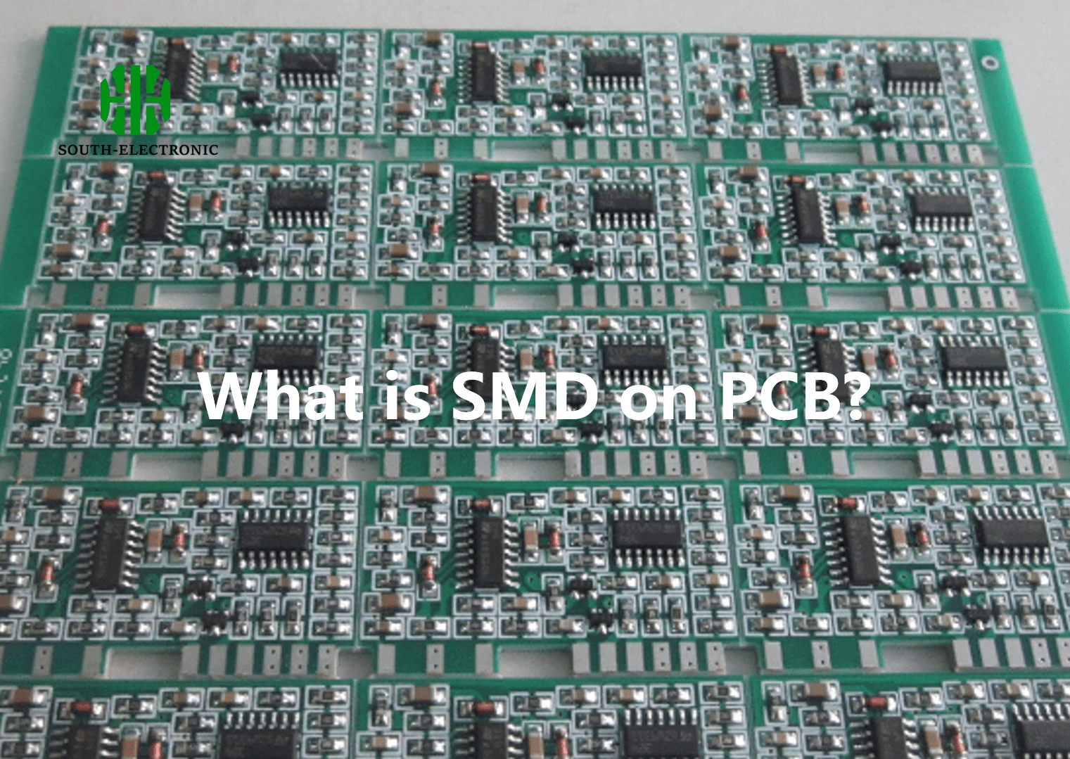
What is SMD on PCB?
SMD stands for “surface-mounted devices” which refers to the components used in surface-mount technology (SMT). Therefore, SMD can also be referred to as SMC (surface-mounted components).
SMD allow for more PCB space because no holes need to be drilled and both sides of the board can be used. You don’t have to worry about any wires going through the board. SMD don’t have any wires, or they may have very small wires.
Applications Across Industries
SMD technology has a wide range of applications in various industries including telecommunications, automotive, consumer electronics, medical devices and aerospace. Its versatility allows the integration of various components such as resistors, capacitors, diodes, transistors and integrated circuits into complex electronic systems.
In summary, SMD technology represents the cornerstone of modern PCB design and manufacturing, providing unparalleled advantages in miniaturization, performance, reliability and production efficiency. As technology continues to develop, SMD is expected to play an increasingly important role in shaping the future of electronic products, driving innovation and meeting the growing demand for smaller, smarter and more efficient electronic devices.
Difference Between SMD and SMT
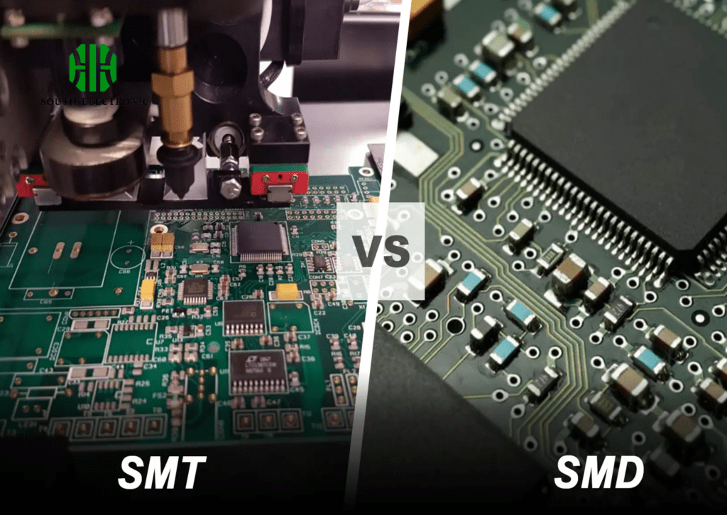
If you are in the circuit board electronics industry, I am sure you must have heard of these two acronyms: SMD and SMT. Spelling-wise, they differ only in letters. However, in reality, they are worlds apart.
SMD (Surface Mount Device):
- Refers to a type of electronic component designed for surface mounting directly onto a PCB.
- Examples include resistors, capacitors, integrated circuits, etc., which are specifically manufactured for surface mounting without the need for leads passing through the PCB.
SMT (Surface Mount Technology):
- Encompasses the entire process of mounting and soldering surface mount components onto a PCB.
- Involves techniques such as solder paste printing, component placement, reflow soldering, and inspection.
- Includes SMD as well as other surface mount components like QFN (Quad Flat No-leads) and BGA (Ball Grid Arrays).
Therefore, SMT is a technology, while SMD is a component. Surface mount technology (SMT) is the process of placing electronic components on PCB. SMD is a surface mount component suitable for SMT PCB assembly.
Characteristics of SMD(Surface Mount Device)
- Size: SMDs are generally smaller in size compared to through-hole components, allowing for higher component density on the PCB.
- Mounting: They are designed for direct mounting on the PCB surface, without the need to drill holes in the board
- Connection: There are metallized terminals or pads under the SMD, which can be directly soldered to the PCB pads during assembly.
- Performance: They provide better high-frequency performance due to shorter lead lengths and reduced parasitic capacitance and inductance.
- Automation: SMDs are compatible with automated assembly processes, such as pick-and-place machines, thus simplifying manufacturing and reducing production costs.
- Heat dissipation: SMDs are typically mounted closer to the PCB surface, which enhances heat dissipation compared to through-hole components.
- Applications: SMDs are widely used in consumer electronics, telecommunications, automotive, medical devices and other industries that require compact, lightweight and high-performance electronic components.
These characteristics make SMD an integral part of modern PCB design and manufacturing, enabling smaller and more efficient electronic devices.
Advantages of SMT(Surface Mount Technology)
Surface mount technology (SMT) offers several advantages compared to traditional through-hole technology (THT), making SMT the first choice for modern electronics manufacturing:
- Size and weight reduction: SMT assembly density is high, because electronic products can be designed to be smaller and lighter, so the volume of the circuit board will also be reduced. This miniaturization helps in the development of smaller and lighter electronic devices.
- Improved Electrical Performance: It has excellent high-frequency characteristics, and SMT components have shorter leads and smaller parasitic capacitance and inductance, which improves high-frequency performance and signal integrity and reduces electromagnetic and radio frequency interference.
- Increase productivity: SMT is easily automated, and it minimizes the need to drill holes in PCBs, simplifying the manufacturing process and thus reducing overall production costs.
- Expand application fields: Using SMT technology, we can design more high-end products and apply electronic products to more fields, such as CPUs, smart phones, etc.
- Automated Assembly: SMT is more suitable for mass production because SMT technology replaces manual plug-in operations with automation and uses placement machines to mount electronic components. Therefore, it is more suitable for mass production of high-quality products with more stable quality.
Overall, the advantages of SMT make it an indispensable technology for achieving high-performance, compact and cost-effective electronic products in today’s competitive market.
Cross-industry Applications of SMD
SMD technology has a wide range of applications in various industries:
- Consumer Electronics: Smartphones, tablets, laptops, wearables, and other consumer gadgets benefit from SMDs’ compact size and high performance.
- Telecommunications: SMDs enable the development of advanced communication devices and infrastructure, supporting faster data transfer and network reliability.
- Medical Devices: Medical equipment relies on SMDs for precise control systems, diagnostics, imaging devices, and implantable electronics.
- Automotive: SMDs enhance automotive electronics, including engine control units (ECUs), infotainment systems, and safety features like airbag sensors and collision detection systems.
- Aerospace and Defense: SMD technology is crucial for aerospace applications, providing lightweight and reliable components for satellites, avionics, and defense systems.

Environmental and Sustainability Considerations
SMD technologies promote environmental sustainability by:
- Reduced Material Waste: SMDs minimize material waste during production compared to THT, supporting eco-friendly manufacturing practices.
- Energy Efficiency: Smaller PCB sizes and efficient design layouts reduce energy consumption in electronic devices.
- Lead-Free Options: Many SMD components use lead-free solder materials, aligning with global environmental regulations and reducing environmental impact.
Challenges and Future Trends
Despite its many advantages, SMD technology still faces the following challenges:
- Miniaturization Limits: Continued demand for smaller devices pushes the limits of component miniaturization and manufacturing precision.
- Thermal Management: Efficient heat dissipation remains crucial for maintaining SMD component reliability, especially in high-power applications.
- Component Reliability: Ensuring long-term reliability and durability of SMD assemblies under varying environmental conditions and operational stresses.
Future trends in SMD technology include advances in materials science, integration of heterogeneous materials, the development of flexible and wearable electronics, and further automation of the assembly process.
Surface mount devices (SMDs) have revolutionized the electronics manufacturing industry, making electronic devices smaller, more efficient, and more reliable across a wide range of industries. As technology continues to advance, SMDs will play a key role in driving innovation, enhancing connectivity, and meeting the evolving needs of the global market. Adopting SMD technology not only accelerates product development, but also contributes to sustainable and environmentally friendly practices in the electronics manufacturing industry.
In conclusion, SMDs are the cornerstone of modern electronics, embodying innovation, efficiency, and reliability in the pursuit of technological advancement.
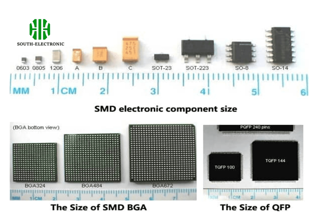
SMD Component Packaging Type
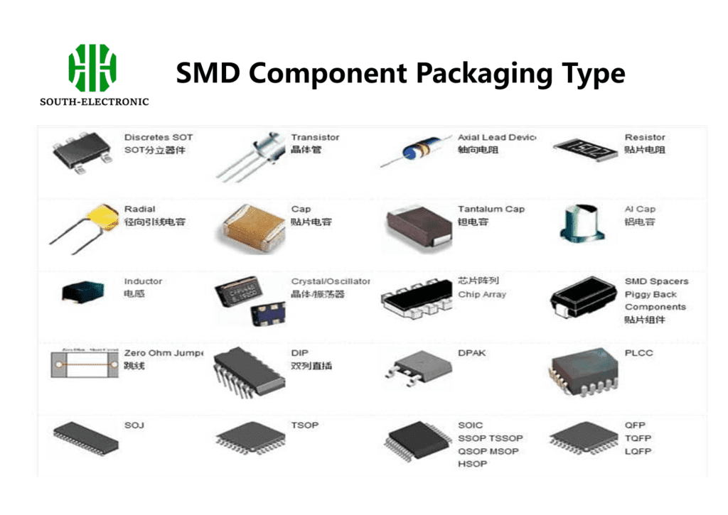
Surface mount devices (SMDs) are available in a variety of package types to suit different applications and performance requirements. These package types ensure compatibility with different assembly processes and PCB design considerations. Here are some common SMD package types:
1.SMD Resistors and Capacitors:
Chip Resistors and Capacitors (0402, 0603, 0805, etc.): These are the smallest SMD components commonly used for basic passive components like resistors and capacitors. They are named based on their dimensions in metric units (e.g., 0402 is 0.4mm x 0.2mm).
2.SMD Diodes and Transistors:
SOT (Small Outline Transistor): Packages like SOT-23, SOT-223, etc., are commonly used for diodes, transistors, and voltage regulators. They offer small size and good thermal management capabilities.
SOD (Small Outline Diode): Similar to SOT packages but specialized for diodes, providing a compact footprint and efficient heat dissipation.
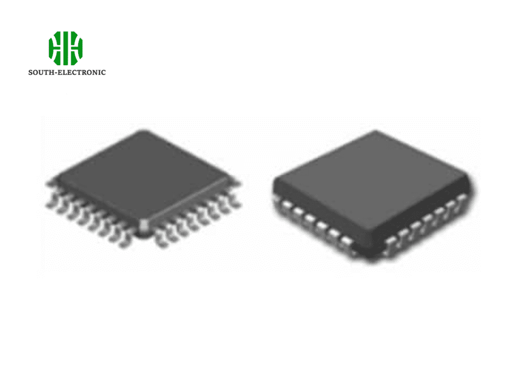
3.SMD Integrated Circuits (ICs):
QFN (Quad Flat No-lead): These packages have no leads and use metal pads on the underside for electrical connections. They provide good thermal and electrical performance and are suitable for high-density applications.
BGA (Ball Grid Array): ICs in BGA packages have solder balls arranged in a grid pattern on the underside of the package. They offer high pin count and excellent thermal dissipation, making them ideal for high-performance applications.
4.SMD Inductors:
Multilayer Ceramic Inductors (MLCIs): These are compact SMD inductors made from multilayer ceramic material. They are used in various RF and power applications due to their high Q factor and stability.
5.Others:
LGA (Land Grid Array): Similar to BGA but with land pads instead of solder balls.
PLCC (Plastic Leaded Chip Carrier): Used for ICs where through-hole mounting is not possible but still require a protective plastic shell.
Each SMD package type has unique advantages in terms of size, thermal management, electrical performance and compatibility with manufacturing processes. Designers choose the appropriate package type based on the specific requirements of the electronic circuit to ensure the best performance and reliability of the final product.
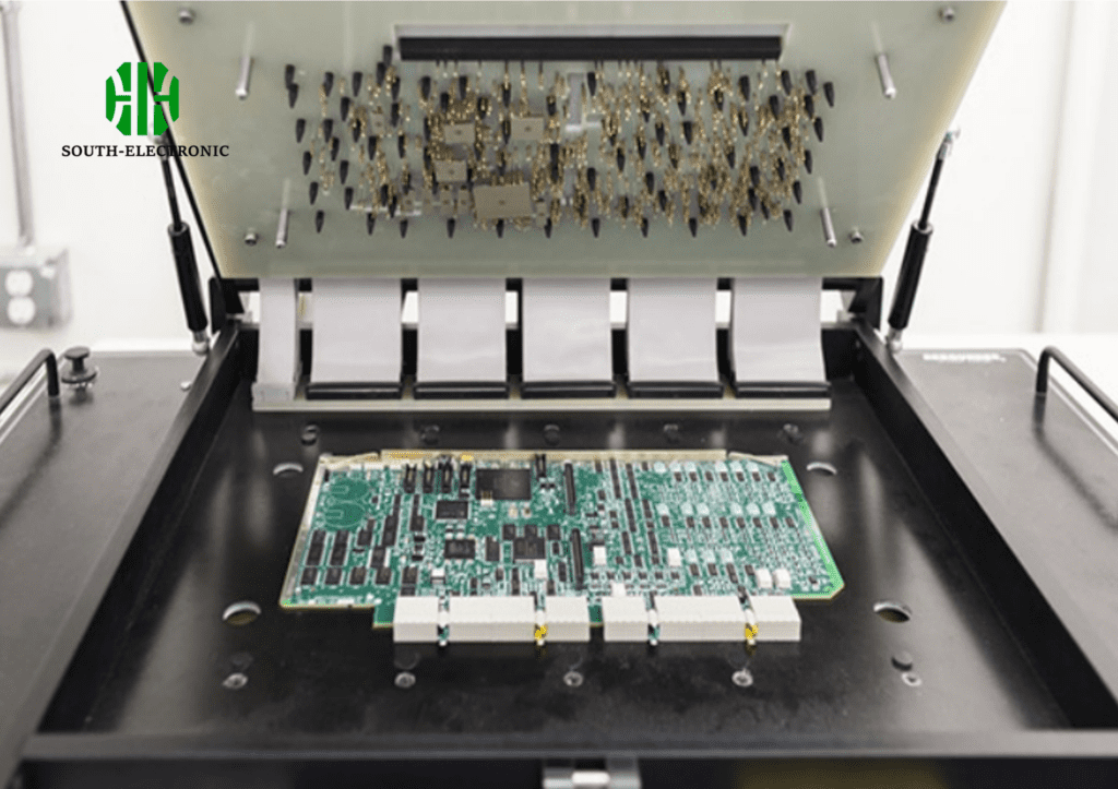
SMD inspection and storage
Inspection of SMDs
1.Visual Inspection:
External Condition: Inspect for physical damage, such as bent leads, cracked packages, or contamination.
Solder Joints: Check solder joints for proper wetting and alignment during assembly.
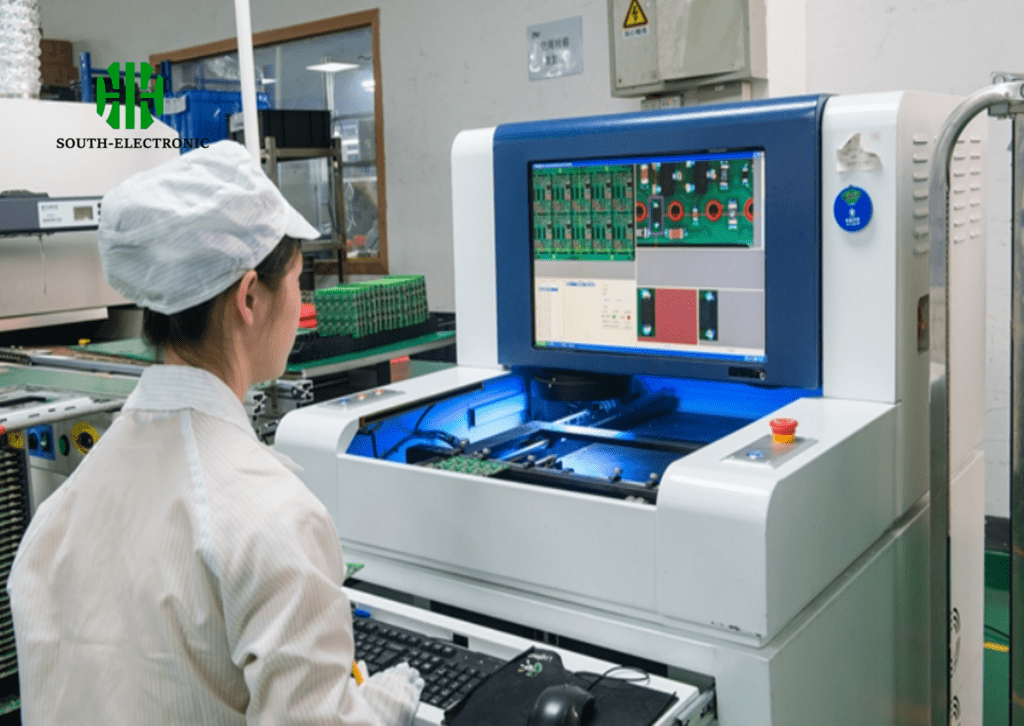
2.Automated Optical Inspection (AOI):
Use AOI systems to detect defects such as misalignment, missing components, solder bridges, or insufficient solder paste.
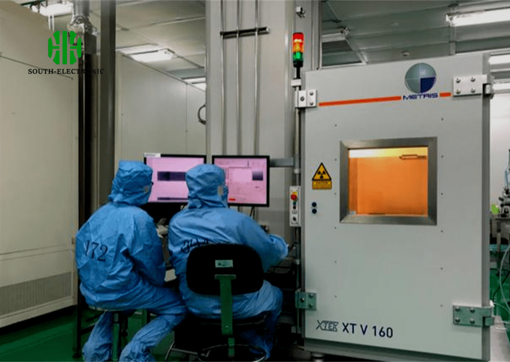
3.X-ray Inspection:
Employ X-ray machines to inspect hidden defects such as voids in solder joints, component misalignment, or internal defects in ICs.
4.Functional Testing:
Conduct functional tests to verify electrical performance and functionality of assembled SMD circuits.
5.Static Electricity Control:
Implement ESD (Electrostatic Discharge) precautions to prevent damage to sensitive SMD components during handling and inspection.
Storage of SMDs
1.Humidity Control:
Store SMDs in controlled environments with low humidity levels to prevent moisture absorption, which can lead to solderability issues and component damage.
Use desiccant packs or humidity-controlled cabinets for long-term storage.
2.Temperature Control:
Maintain stable temperatures within recommended ranges to prevent thermal stress on SMDs.
Avoid rapid temperature fluctuations that can cause condensation inside component packaging.
3.Packaging:
Store SMD components in their original packaging or antistatic packaging to protect against ESD and physical damage.
Use moisture barrier bags for moisture-sensitive devices (MSDs) to maintain proper storage conditions.
4.Labeling and Inventory Management:
Clearly label storage containers with component specifications, quantities, and storage conditions.
Implement a systematic inventory management system to track stock levels, expiration dates (for moisture-sensitive components), and usage history.
5.Handling Practices:
Handle SMD components with care to avoid mechanical damage or ESD. Use ESD-safe equipment and personal protective gear (e.g., wrist straps, grounded workbenches) when handling sensitive components.
Best Practices Summary
Adhere to strict inspection and storage practices to ensure the quality and reliability of SMD components throughout the lifecycle of electronics manufacturing. By maintaining proper environmental controls, using advanced inspection techniques, and implementing ESD protection measures, manufacturers can reduce the risks associated with component defects and ensure consistent performance of electronic assemblies.
In summary, meticulous inspection and storage of SMD components are important steps to achieve high-quality electronic product production. These practices not only safeguard the integrity of components, but also help improve overall manufacturing efficiency and customer satisfaction in the dynamic electronics world.