
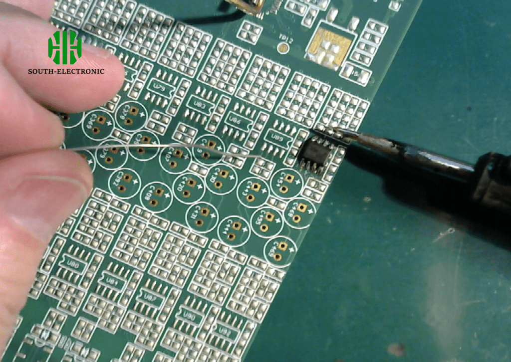
Ever struggled with uneven solder paste distribution[^1] on your PCB? Imagine perfect paste application every time. SMT stencils[^2] solve this exact problem in surface-mount technology manufacturing with surgical precision.
SMT stencils are laser-cut stainless steel templates that precisely deposit solder paste onto PCB pads during the assembly process. These essential tools ensure correct solder volume and placement accuracy for reliable electrical connections in modern electronics.
While SMT stencils might look simple, choosing the right type and using it properly makes the difference between flawless production runs and costly rework. Let’s explore why these tools are non-negotiable in electronics manufacturing and how to optimize their use.
Why Can’t You Skip SMT Stencils in Modern Electronics Manufacturing?
Watch any electronics factory floor – you’ll see stencils everywhere. Why do manufacturers insist on using these metal sheets despite their cost? The answer lies in the cost of not using them.
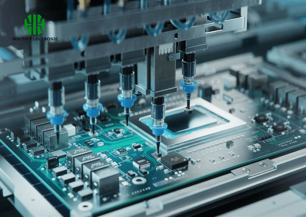
SMT stencils prevent solder bridging[^3] and insufficient joints by controlling paste deposition. Manual application can’t match their 0.01mm precision, making stencils mandatory for components smaller than 0402 size or BGAs with hidden joints.
Three Uncompromising Reasons for Stencil Use
-
Micro-Scale Requirements
Modern components like 01005 chips (0.4mm x 0.2mm) demand paste deposits thinner than human hair. Human hands shake – machines guided by stencils don’t. -
Repeatability Metrics
Automated lines produce 50,000+ boards daily. Without stencils, paste volume would vary ±30% vs ±5% with stencils. -
Cost Analysis
| Scenario | Defect Rate | Rework Cost/Hour |
|---|---|---|
| No Stencil | 15% | $120 |
| Using Stencil | 2% | $20 |
This table explains why manufacturers swallow stencil costs – they actually save millions in reduced defects.
How to Choose Between Framed vs Frameless Stencils for Your Project?
Your stencil choice impacts production flexibility and costs more than you think. Let’s cut through the confusion.
Framed stencils[^4] (mounted in aluminum frames) suit high-volume production needing quick changes. Frameless stencils (bare steel sheets) work better for prototypes and small batches where storage space matters.
)
Decision Matrix for Stencil Selection
Key Differences Table
| Factor | Framed Stencil | Frameless Stencil |
|---|---|---|
| Setup Time | 2 minutes | 15 minutes |
| Unit Cost | $250+ | $80-$150 |
| Minimum Order | 1 piece | 3+ pieces |
| Best For | Full production runs | NPI builds |
When to Choose Framed
- Running 500+ identical boards
- Automated screen printers
- Limited engineering staff
When Frameless Makes Sense
- Testing 5 design iterations
- Budget under $1,000
- Benchtop manual printers
What Are the Critical Stencil Design Rules Professionals Never Ignore?
Bad stencil design causes 73% of solder defects (IPC data). Avoid becoming a statistic by mastering these non-negotiable rules.
Critical rules include maintaining 1:1.5 aperture aspect ratio, using rounded aperture corners, and implementing 85% area ratio minimum. Proper design prevents solder balls and component tombstoning.
Golden Rules for Flawless Printing
1. Aperture Geometry Guidelines
- Round corners reduce paste sticking
- Trapezoidal walls improve release
2. Thickness Selection Chart
| Component Pitch | Stencil Thickness |
|---|---|
| >1.27mm | 150µm |
| 0.65-1.27mm | 130µm |
| <0.65mm | 100µm |
3. Cleaning Protocol
Every 5 prints for no-clean pastes
Every print for water-soluble pastes
Violate these rules and you'll face solder shorts or insufficient joints. I learned this hard way when a 0.4mm pitch QFN design ignored width-to-thickness ratios – entire batch scrapped.
How to Avoid 6 Costly Stencil Mistakes That Ruin SMA Quality?
From stretched apertures to wrong squeegee angles, stencil errors compound through production. Let's eliminate these common pitfalls.
Top errors: ignoring nickel plating for fine-pitch, incorrect aperture size calculations, using damaged stencils, poor cleaning, wrong tensioning, and mismatched solder alloys. All cause SMA (surface mount assembly) failures[^5].
Mistake Breakdown and Solutions
1. Wrong Material Choice
Use electroformed nickel[^6] for <0.5mm pitch vs standard stainless steel
2. Ignoring Fiducial Marks
Include 3 global fiducials for precise alignment
3. Squeegee Pressure Issues
| Symptom | Pressure Adjustment |
|---|---|
| Streaky deposits | Increase 10% |
| Paste bleeding | Decrease 15% |
4. Skipping Step-Downs
For mixed components, use 50µm reductions in dense areas
5. Poor Storage
Hang vertically in climate control (22°C±3, RH<60%)
6. Laser Parameters
Set pulse width <30ns for clean aperture walls
Fix these and watch your first-pass yield jump 27% (industry average).
Conclusion
SMT stencils are precision tools enabling modern electronics. Choosing the right type, following design rules, and avoiding common mistakes ensures reliable, cost-effective PCB assembly from prototype to mass production.
[^1]: Learn about the critical role of solder paste distribution in PCB assembly and how it impacts overall product reliability.
[^2]: Explore this link to understand how SMT stencils enhance precision and efficiency in PCB manufacturing, ensuring high-quality electronics.
[^3]: Discover effective strategies to prevent solder bridging, a common issue in PCB assembly that can lead to costly defects.
[^4]: Explore the benefits of framed stencils for high-volume production and quick changes, enhancing your project efficiency.
[^5]: Understanding the causes of SMA failures can help you avoid costly mistakes in PCB assembly.
[^6]: Learn about electroformed nickel’s benefits for fine-pitch applications to enhance your PCB assembly quality.


