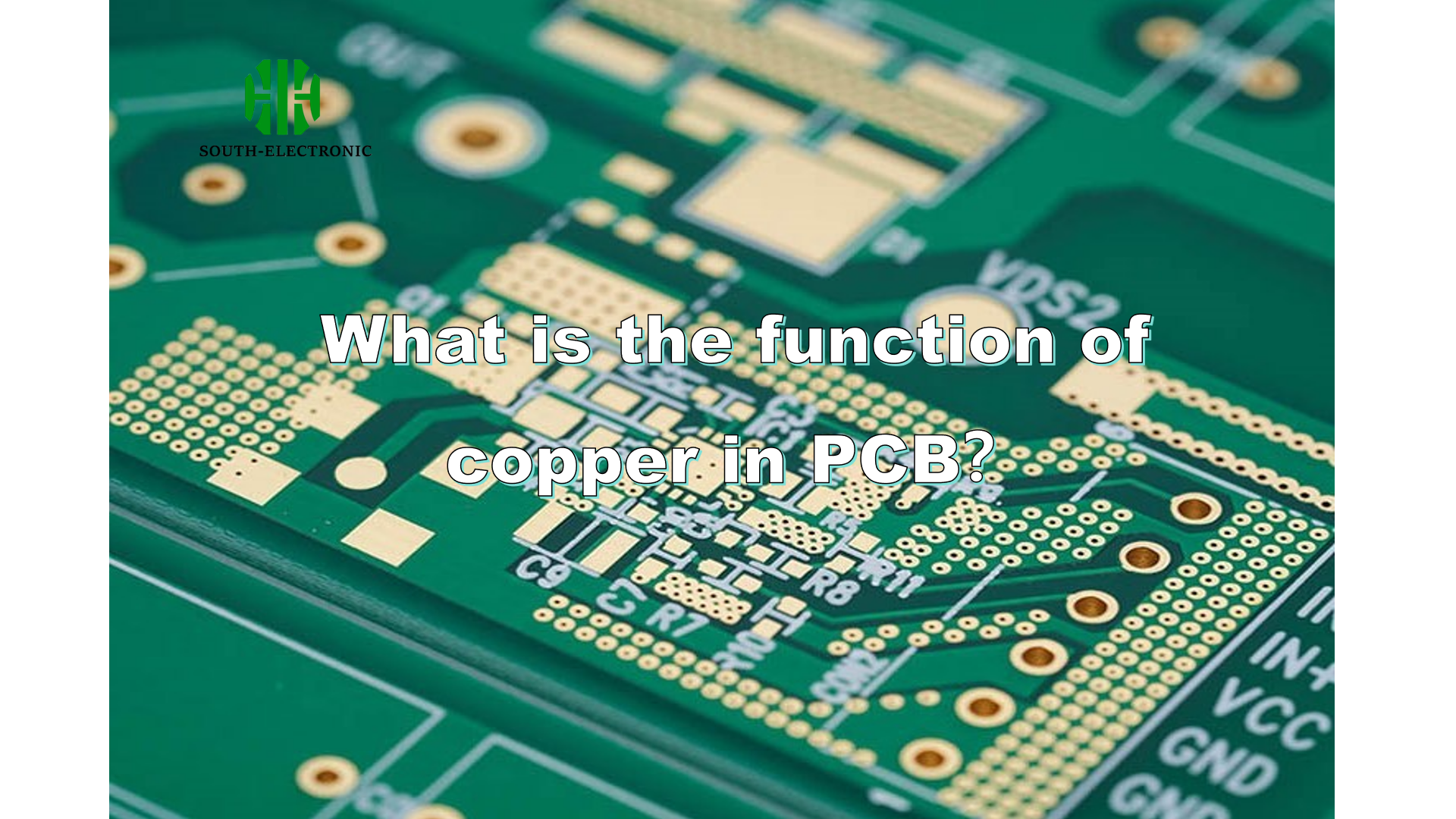
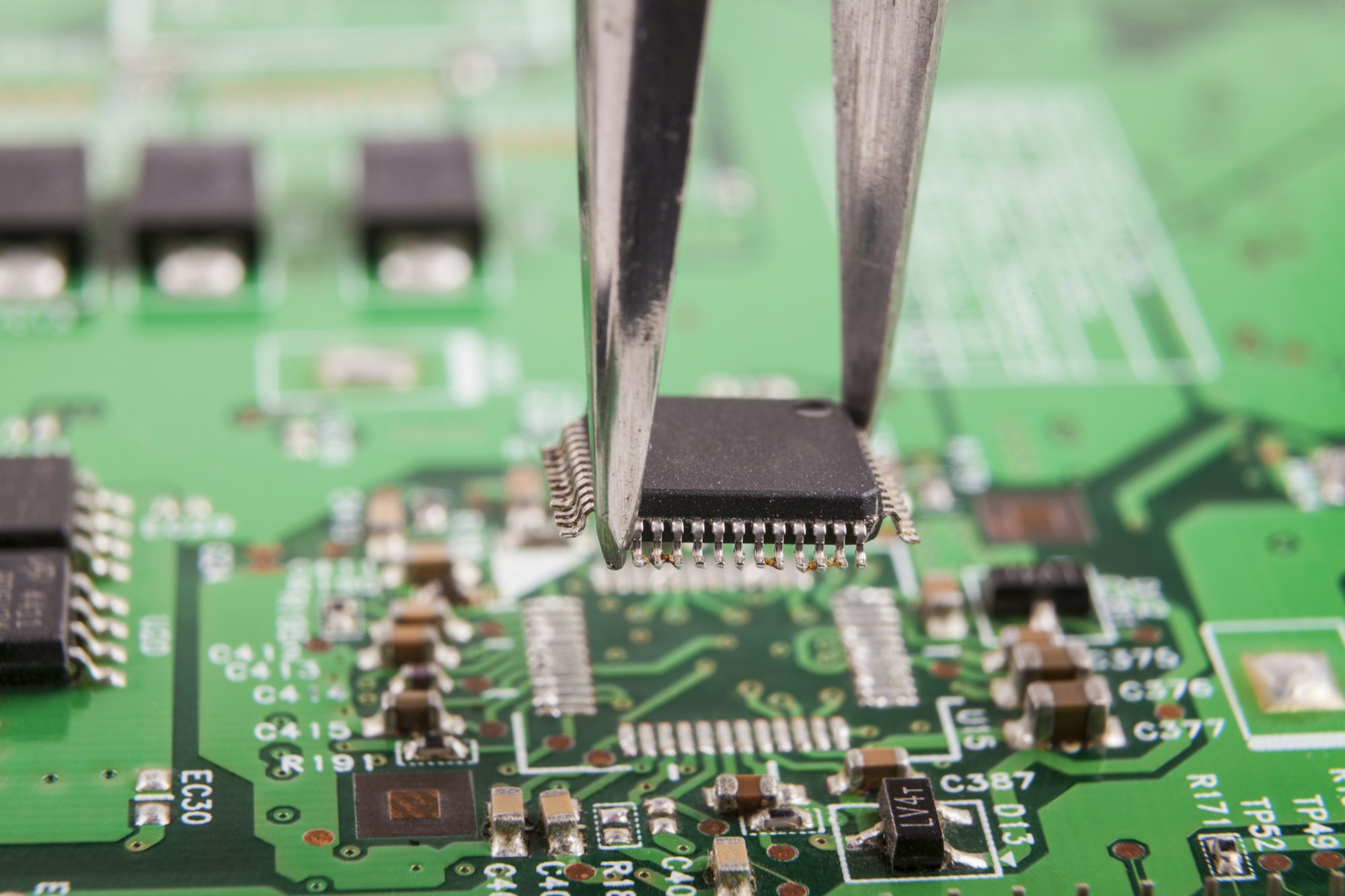
What is the function of copper in printed circuit boards?
To understand what’s the function of copper in PCB, let us make it clear here:
Printed circuit boards are composed of many layers and components, including circuits, characters, metal layers, and other materials. Circuits are the connecting components of PCBs, because without circuits, no charge flow occurs, so we can say that circuits act as blood vessels in the bones of PCBs, and without circuits, no PCB can function properly. Without PCBs, there is no concept of electronic devices. In this day and age, every device is using PCBs. Compared with other components, PCBs rely most on copper because copper helps to form lines. The reason for using copper is its conductivity. The conductivity of copper metal ensures that the transmission speed of signals in electronic devices is not interrupted. The reason for the high conductivity of copper is that it has only one electron in its valence layer. This one electron can easily move from one atom to another without any resistance. This is why copper can carry charge without losing the signal.
To make continuous metal foil, copper, which is a negative electrolyte, is used on the first layer of the PCB. Due to the low level of surface oxygen; copper can be easily used in various types of substrates, metals, and insulating layers. Copper is used with a protective layer after etching to form different circuit patterns because it can easily bond with the insulating layer of the PCB. Copper foil can provide better continuity of electromagnetic shielding, that is why it is placed on the surface of the substrate board.
There are some things you have to know about “balanced copper” in PCB
PCB manufacturing is the process of building a physical PCB from a PCB design following a set of specifications. Understanding the design specifications is very important as it affects the manufacturability, performance, and production yield of the PCB.
One of the important design specifications to follow is “balanced copper” in PCB manufacturing. Consistent copper coverage must be achieved in each layer of the PCB stack-up to avoid electrical and mechanical issues that can hinder circuit performance.。
What does PCB balanced copper mean?
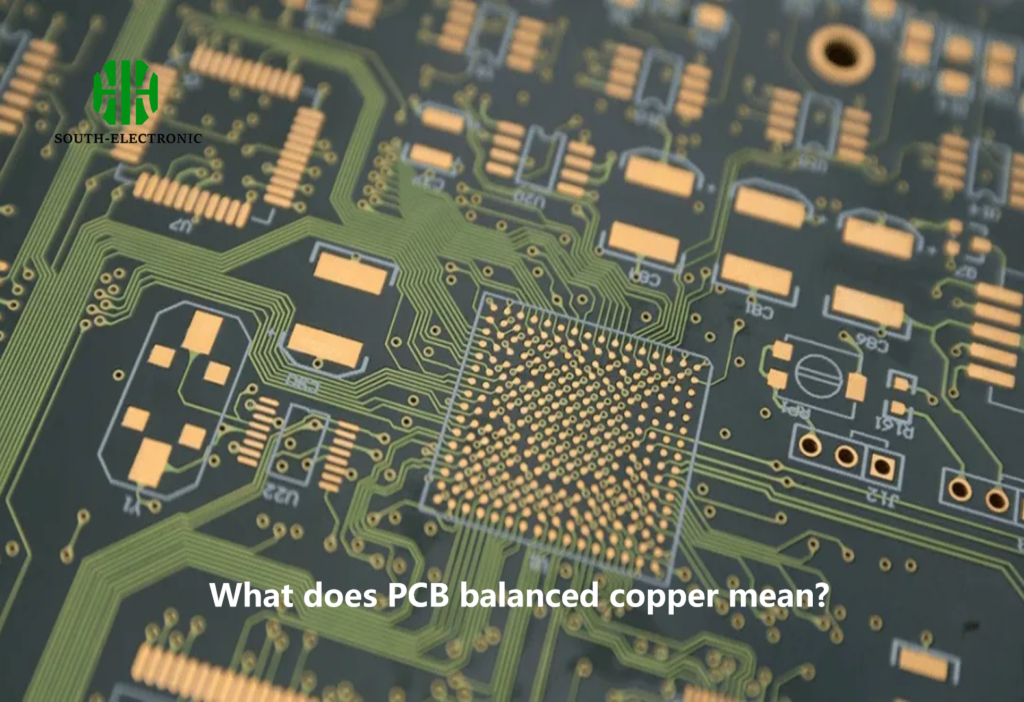
Balanced copper is a method of symmetrical copper traces in each layer of the PCB stack-up, which is necessary to avoid twisting, bending, or warping of the board. Some layout engineers and manufacturers insist that the mirrored stack-up of the top half of the layer be perfectly symmetrical with the bottom half of the PCB.
The function of balanced copper:
- Routing:The copper layer is etched to form the traces, and the copper used as the traces carries the heat along with the signal throughout the board. This reduces damage from irregular heating of the board that could cause internal tracks to break.
- As a heat sink:Copper is used as a heat dissipation layer for the power generation circuit, avoiding the use of additional heat dissipation components and reducing manufacturing costs to a great extent.
- Increase the thickness of conductors and surface pads:Copper used as plating on PCBs increases the thickness of conductors and surface pads. In addition, plated through-holes provide a strong copper connection between layers.
- Reduces ground line impedance and voltage drop:PCB balanced copper reduces ground line impedance and voltage drop, thereby reducing noise, while at the same time improving the efficiency of the power supply.
What issues arise from uneven copper distribution in PCB stack-up layers?
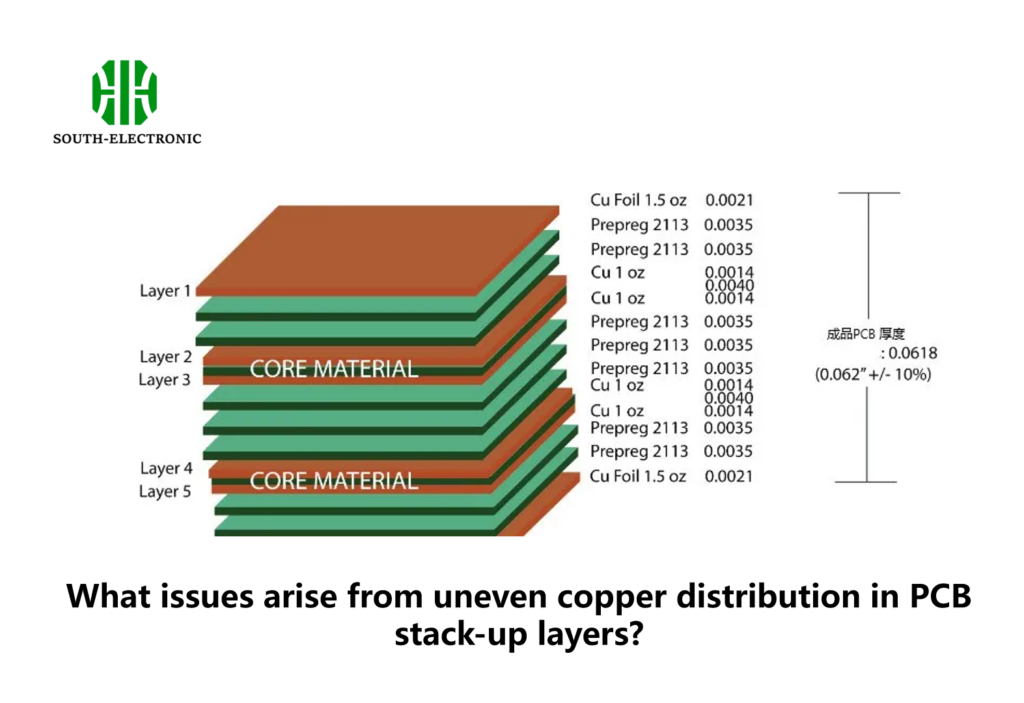
In PCB manufacturing, if the copper distribution between stack-up layers is uneven, the following problems may occur:
1、Improper stack balance
A balanced stack means having symmetrical layers in your design, the idea being to forgo risky areas that could deform during the stack-up assembly and lamination stages.
The best approach is to start the stack-up design from the center of the board and place the thick layers there. Often, the strategy among PCB designers is to mirror the top half of the stack-up with the bottom half.
2、PCB will delaminate
The problem mainly comes from using thicker copper (50um or more) on the core where the copper surface is unbalanced, and worse, there is almost no copper fill in the pattern.
In this case, the copper surface needs to be supplemented with “dummy” areas or planes to prevent the prepreg from overflowing into the pattern and subsequent delamination or inter-layer shorts.
No PCB delamination: 85% of the copper is filled in the inner layers, so filling the prepreg is enough and there is no risk of delamination.
There is a risk of PCB delamination: copper filling is only 45%, and the prepreg between layers is insufficient, so there is a risk of delamination.
3、Uneven dielectric layer thickness
Layer stack-up management is a key element in designing high-speed boards. To maintain the symmetry of the layout, the safest practice is to balance the dielectric layers, and the dielectric layer thickness should be arranged symmetrica
4.The cross section of the circuit board is uneven
One of the common unbalanced design issues is improper board cross-section. Copper deposition is greater in some layers than in others. This problem stems from the fact that copper consistency is not maintained across the different layers. As a result, upon assembly, some layers become thicker while other layers with low copper deposition remain thinner. When pressure is applied laterally to the board, it deforms. To avoid this, the copper coverage must be symmetrical with respect to the center layer.
5.Hybrid (mixed material) lamination
Sometimes, designs use mixed materials in the roof layer. Different materials have different thermal coefficients (CTC). This type of mixed structure increases the risk of warping during reflow assembly.
Effects of Copper Deposition Variations
Variations in copper deposition can cause PCB warping. Some of the warping and defects are mentioned below:
1、Warping Warping is nothing but a deformation of the board shape.
During the baking and handling of the board, the copper foil and substrate undergo different mechanical expansion and compression. This causes deviations in their coefficients of expansion. Subsequently, the internal stresses generated in the board cause warping. Depending on the application, the PCB material can be fiberglass or any other composite material. During the manufacturing process, the board undergoes multiple heat treatments. If the heat is not evenly distributed and the temperature exceeds the thermal expansion coefficient (Tg), the board will warp.
2、Poor electroplating of conductive patterns
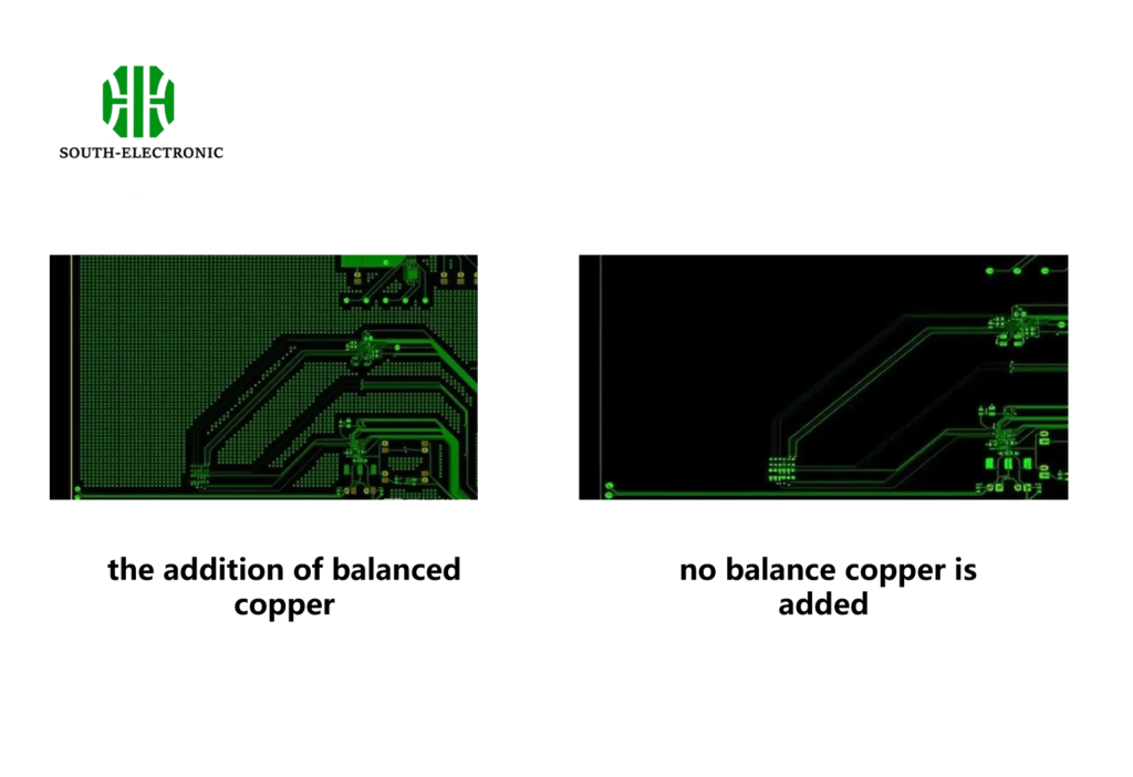
In order to correctly set up the electroplating process, copper balance on the conductive layer is very important. If the copper is not balanced on the top and bottom, or even on each individual layer, overplating occurs and leads to connected tracks or under-etching. In particular, this involves differential pairs with measured impedance values. Setting up a correct electroplating process is complicated and sometimes impossible. Therefore, it is important to supplement the copper balance with “dummy” patches or full copper.
3、Bow
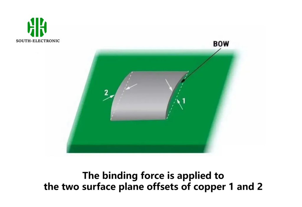
If the copper pour is not balanced, the PCB layer will have a cylindrical or spherical curvature. In simple language, you can say that the four corners of a table are fixed and the top of the table rises above. It is called bow and is the result of a technical malfunction. Bow creates tension on the surface in the same direction as the curve. Moreover, it causes random current flow through the board.
PCB Balanced Copper Design Specifications
Therefore, the following PCB balanced copper design specifications should be followed
- During stack-up design, it is recommended to set the center layer to the maximum copper thickness and further balance the remaining layers to match their mirror image opposite layers. This recommendation is important to avoid the potato chip effect discussed earlier.
- Where there are wide copper areas on the PCB, it is wise to design them as a grid rather than a solid plane to avoid mismatched copper density in that layer. This largely avoids bow and twist issues.
- In the stack-up, the power layers should be placed symmetrically and the copper weight used in each power layer should be the same.
- Copper balancing is not only necessary in the signal or power layers, but also in the core and prepreg layers of the PCB. Ensuring an even ratio of copper in these layers is a good way to maintain the overall copper balance of the PCB.
- If there are excess copper areas in a particular layer, the symmetrical opposite layer should be filled with tiny copper grids to balance. These tiny copper grids will not be connected to any net and will not interfere with the function. But it is necessary to ensure that this copper balancing technique does not affect the signal integrity or board impedance.
Copper in PCBs ensures signal conductivity, heat dissipation, and structural integrity. Balanced copper design avoids issues like warping, delamination, uneven dielectric layers, and improper electroplating. To prevent defects, symmetrical copper distribution is essential across all PCB layers, including power, signal, and core layers.

