
Ever wrestled with a loose cable or glitchy device? Faulty connections ruin electronics daily. This problem plagues billions worldwide.
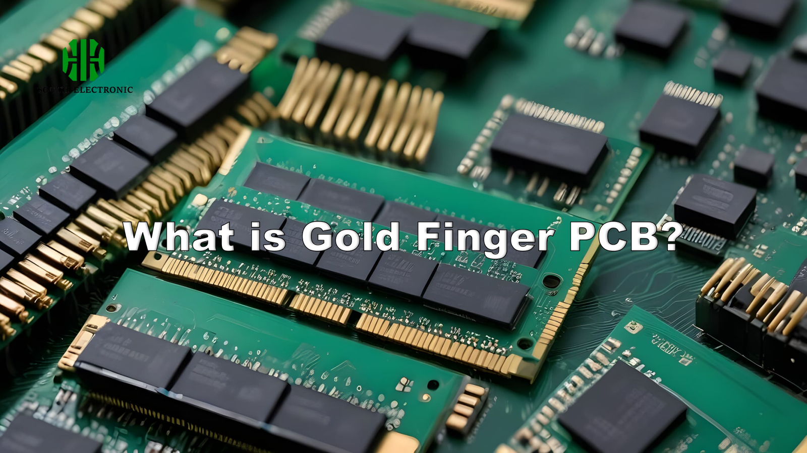
Gold finger technology uses gold-plated edge connectors on PCBs to create corrosion-resistant, high-conductivity contacts between electronic components. It ensures reliable signal transmission and physical stability in devices like computers and medical equipment. Gold prevents oxidation better than copper or silver.
Now, let’s uncover the specifics that make this technology work so effectively across industries.
How thick and angled should PCB gold fingers be?
Sloppy dimensions cause insertion failures. Imagine your RAM stick refusing to seat properly. Frustration awaits!
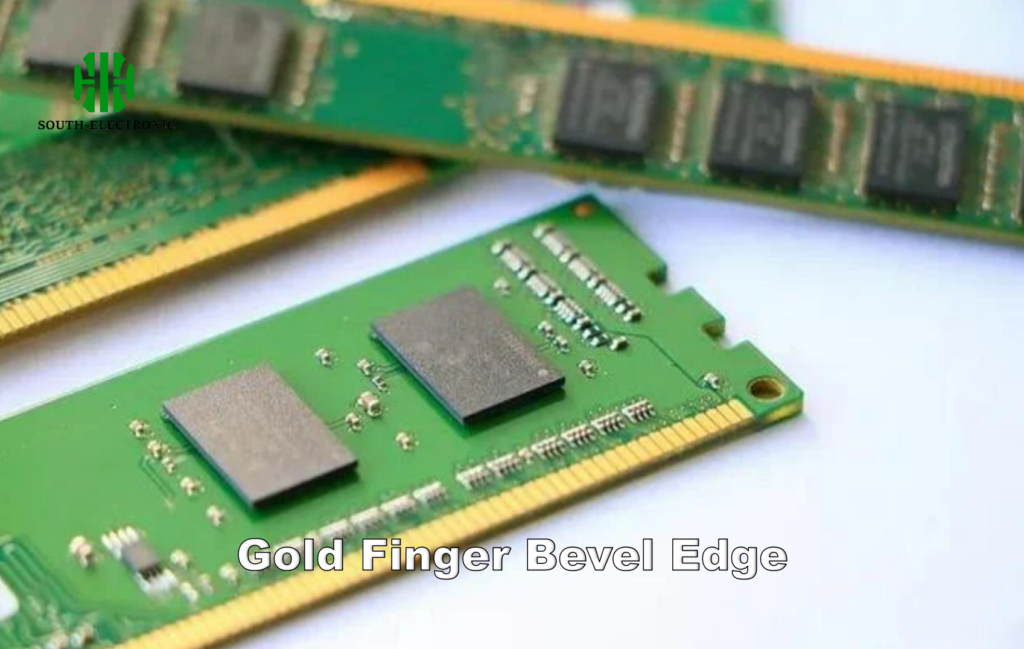
Standard gold plating should be 0.3–1.27μm thick for durability, with a 30° or 45° beveled edge. Common angles match slot designs while reducing wear.

Dimensions in Practice
Proper thickness prevents scraping during mating cycles, while angled edges guide insertion. Three elements dominate this decision:
Thickness Standards
| Use Case | Optimal Thickness | Why It Matters |
|---|---|---|
| Light-Duty Devices | 0.3–0.5µm | Cost-efficient for low cycles |
| General Electronics | 0.8µm | Balances wear and budget |
| Military/Servers | 1.27µm | Withstands intense friction |
Angle Selection
30° angles fit most card slots. 45° suits tight-space applications like stacked PCBs. Angling reduces stress by minimizing perpendicular forces.
Impact of Errors
Too thin? Gold flakes off after 50+ cycles. Too steep? Connectors jam or fracture. Engineers balance IPC-6013 standards against hardware needs. Most failures trace to ignoring these specs.
What types and alternatives exist for PCB gold fingers?
Not all connections demand pure gold. Some materials spark disasters in humid factories. Know your options!
Hard gold (electroplated) suits high-wear slots like PCIe. Soft gold (ENIG) works for solderable joints. Alternatives include palladium-nickel and selective tin.
Comparing Solutions
We weigh conductivity, costs, and longevity. Here’s how they differ:
Core Materials
- Hard Gold: Pure cobalt-hardened gold. Best for memory slots where durability matters. Higher-cost but lasts 10,000+ cycles.
- Soft Gold: Contains nickel beneath gold layers. Cheaper yet prone to scratches. Ideal for solder pads.
- Palladium-Nickel: More rigid than gold, resisting micro-cracks. Often used in automotive boards.
Alternative Tradeoffs
| Material | Conductivity | Corrosion Resistance | Cost vs Gold |
|---|---|---|---|
| Tin-Lead | Moderate | Poor | 60% Cheaper |
| Palladium-Nickel | High | Excellent | 25% Costlier |
| Silver Polymer | High | Unstable in humidity | 40% Savings |
Practical Choices
For prototype PCBs, I choose tin. For server racks? Only hard gold handles constant swapping. Cheaper materials degrade fast in salty/humid air. Always match material to environment.
Are gold fingers necessary for all PCBs?
Stop wasting gold on gadgets doomed for landfills! Non-critical boards thrive cheaper. But some must have it.
Most PCBs without hot-swapping function fine using copper pads. Gold shines only for removable connections. Still, skipping it risks failure in cars or servers.

Evaluating Requirements
Three conditions determine if gold is essential:
Critical Applications
- Edge Connectors: PCIe, RAM modules, etc. Gold’s friction tolerance prevents wear.
- Extreme Envronments: Medical tools face sterilization chemicals. Gold maintains surface integrity.
- Rapid Plugging: Test equipment connectors need daily swaps. Gold plating survives 10× longer than tin.
Where Alternatives Win
| Scenario | Suitable Material | Reasoning |
|---|---|---|
| Fixed Internal Boards | ENIG or HASL | Zero repeated contact |
| Low-Cost Toys | Copper w/coatings | Short lifespan priority |
| Temporary Prototypes | Bare Nickel/Tin | Recyclable/disposable |
Key Decision Points
I recommend gold for any PCB encountering frequent physical stress or corrosive elements. Simple IoT sensors? Tin suffices. Analyze insertion cycles and environmental exposure to cut unnecessary costs.
Conclusion
Gold fingers deliver unmatched reliability where connectivity matters most—balance their cost against application demands for smarter electronics design.

