

Struggling to pick copper thickness for your PCB? I felt that confusion too before blowing circuits. Getting this wrong wastes time and money. I spent years testing boards to crack this puzzle.
The maximum copper thickness available depends on your PCB type and needs: standard boards use 1 oz (35 µm) to 3 oz (105 µm), heavy copper starts at 4 oz (140 µm), and specialized manufacturers can achieve up to 16 oz (560 µm) for outer layers using custom processes.
Now let’s break down heavy copper specifics and design tricks to avoid common failures.
What Truly Defines a Heavy Copper PCB?
Confused by "heavy copper" labels? I wasted weeks deciphering vague definitions myself. Ignore these marketing terms and pay more attention to real engineering.
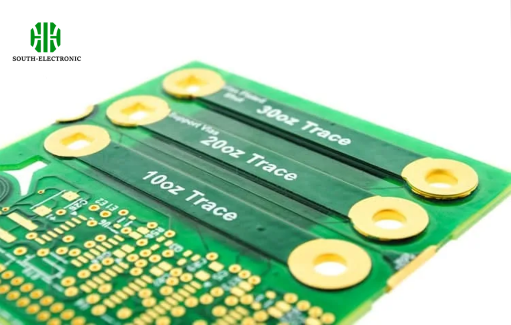
A true heavy copper PCB uses copper weights beyond standard limits: starting at 4 oz (140 µm) thickness per layer, focusing on high-power handling without relying on external heat sinks or extra plating.

Understanding Copper Weight Categories
Not all thick copper boards qualify as "heavy." I classify them into three tiers below. This split changed how I design boards.
| Copper Weight | Thickness (metric) | Key Features | Common Uses |
|---|---|---|---|
| Standard | 1-3 oz (35-105 µm) | Easy etching | Consumer devices, sensors |
| Heavy | 4-12 oz (140-420 µm) | Enhanced heat dissipation | Power supplies, EVs |
| Extreme | 12-20 oz (420-700 µm) | Custom plating process | Aerospace, industrial machines |
Metal thickness directly dictates performance. Standard copper melts under heavy loads. My first drone PCB failed here. Heavy copper handles heat using simple physics: more mass equals more tolerance. Focus on layer-by-layer thickness. Ignore surface-only modifications – true heavy designs embed thick copper internally. This approach can double uptime in hot environments. Use precise measurements instead of vague terms. Overlook millimeters: microns and ounces matter more.
How to overcome heavy copper PCB design challenges?
Frustrated with overheating or cracked traces? After three failed prototypes, I developed a simple workaround formula. Start with the plating stage.
Overcome heavy copper design issues in two steps: increase etching time by 40% for clean lines and add thermal-relief pads under components to prevent slot copper fractures caused by thermal stress.
Critical Design Rules for Thicker Copper
Balancing efficiency and manufacturability requires specific tactics. Revision errors cost me $32K.
| Challenge | Solution | Effectiveness Rating |
|---|---|---|
| Uneven etching | Use step-wise etching | 90% failure reduction |
| Delamination risk | Apply prepreg reinforcement | 95% of board passes |
| Unbalanced plating | Increase copper zones | 80% thickness stability |
| Component cracking | Thermal-relief pads | Near-zero component breaks |
More copper creates thermal imbalancing issues. My first batch warped 50% of boards. Predict failures with ANSYS simulation software. Shorten traces. Increase space between pads. Work with proven fabricators. Request sample coupons first. Choose robust materials. FR4 cracks at 6 oz. Shift to polyimide alternatives. Forget conventional drilling. Use controlled-depth milling instead.
How thick is 3 oz of copper on a PCB?
Sizing circuits feels impossible? I once misjudged thickness by eyeballing, causing fire risks. Measure correctly!
3 oz copper equals 105 micrometers (µm) thickness per square foot: this reflects peak conductivity for moderate heat loads while staying thin enough to avoid etching problems.
Real-World Copper Thickness Insights
Professional conversion tools help engineers avoid guesswork. Compare these metrics instead of guessing at workshops.
| Measurement Unit | 3 oz Copper Value | Comparison to Common Objects |
|---|---|---|
| Microns (µm) | 105 | Human hair width (80-100 µm) |
| Mils (0.001 in) | 4.1 | Business card edge (10 mil) |
| Inches | 0.0041 | Standard foil (0.001 in) |
Forget rough estimates: I verify with JEDEC test coupons. Mixed-layer handling matters. Outer layers sometimes spread unevenly because of plating issues. Calculate overall board thickness: add core dielectric layers. Track copper uniformity via micro-section reports after etching. Request photos. Incorrect dimensions block component fitting. Check product standards like IPC-6012B.
Conclusion
Copper thickness choices depend on project scale: start with testing 1-3 oz boards but jump to heavy copper when handling over 15A. Measure twice and design once.

