
What is the Most Difficult PCB You Have Ever Designed?
Creating the hardest PCBs means dealing with many layers, complex circuits, and making sure signals don’t get messed up while also dealing with heat and EMI. You need some serious tools, some serious planning, and some serious problem-solving skills to make a board that works and keeps on working.
Let’s delve into the complexities and strategies employed in creating a challenging PCB design.
My Journey as a PCB Designer
My journey in PCB design started with basic single-layer boards and progressively moved to more complex multi-layer designs. Over the years, I have used various tools, including Eagle and Altium Designer, which have equipped me with the skills necessary to tackle increasingly challenging projects.
Specific Challenges in the Most Difficult PCB Design
High-Density Circuit Layout
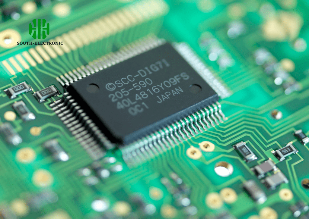
One of the biggest challenges in designing complex PCBs is managing space while making sure components are placed in the best possible way. When you have a lot of circuitry packed into a small space, you have to plan everything out carefully to make sure signals stay clean, especially in high-speed circuits.
Heat Dissipation and Thermal Management
Getting rid of heat is super important in tightly packed circuit boards. You gotta use things like thermal vias, heat sinks, and the right materials to keep things cool and avoid heat problems.
Electromagnetic Interference (EMI) Mitigation
Reducing electromagnetic interference is another big challenge. Shielding and grounding techniques are key to reducing EMI and making sure the board works right.
EMI Shielding Materials and Their Properties
| Material | Conductivity | Permeability | Applications |
|---|---|---|---|
| Copper | High | Low | General shielding |
| Aluminum | Medium | Low | Lightweight applications |
| Nickel | Medium | High | High-frequency shielding |
| Conductive Foam | Low | Low | Flexible shielding |
Solutions and Techniques Employed
Advanced PCB Design Techniques
To tackle these challenges, I used advanced PCB design techniques like blind and buried vias and implemented differential pair routing for high-speed signals.
Design for Manufacturability (DFM) Considerations
Making sure the PCB design can be manufactured without sacrificing performance is key. That means working closely with manufacturers to tweak design elements and follow manufacturing constraints.
Outcome and Results
Performance Testing and Validation
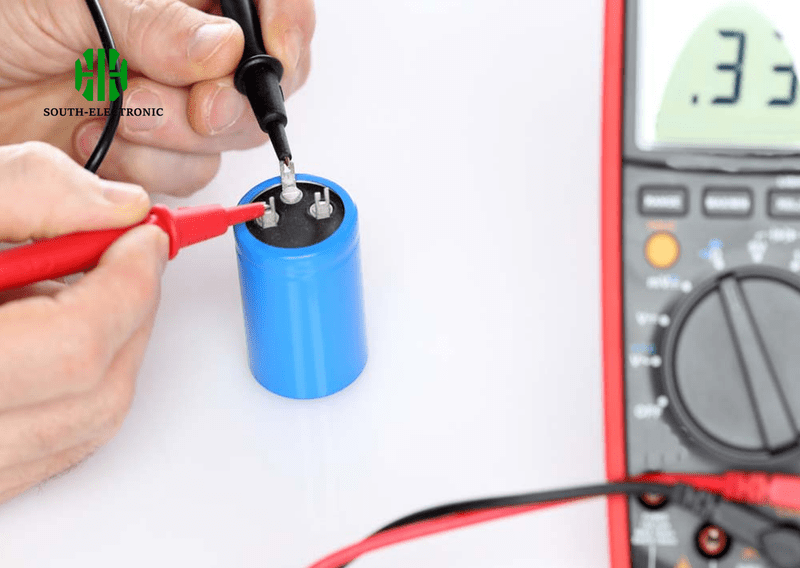
I tested the final PCB like crazy to make sure it worked. I ran all kinds of tests to check the signal quality, how hot it got, and whether it messed with other stuff nearby. Everything looked great.
Lessons Learned
The experience was a great learning opportunity, and it taught me the importance of planning, problem-solving, and always learning. My advice to other PCB designers is to stay up-to-date on the latest tools and techniques, and never underestimate the value of collaboration and testing.
Summary
In short, designing complex PCBs is tough but worth it. The main challenges are high-density layout, heat, and EMI. You can handle these challenges by using advanced techniques and working closely with manufacturers.
Key Challenges and Solutions in Complex PCB Design
| Challenge | Solution | Tools/Techniques |
|---|---|---|
| High-Density Layout | Optimized component placement | Advanced CAD tools |
| Heat Dissipation | Use of thermal vias and heat sinks | Thermal simulation software |
| Electromagnetic Interference | Shielding and grounding techniques | EMI analysis tools |
Creating complex PCBs is a tough but rewarding task that stretches your engineering creativity and technical skills. If you know the challenges and apply the right solutions, you can make efficient, reliable, high-performance PCB designs.


