
Your smartphone’s brain hides a secret: paper-thin layers[^1] transform chaos into order through heat and crushing force. If it fails, your device becomes scrap. How does this invisible welding work?
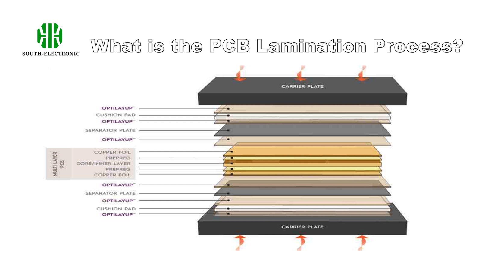
PCB lamination bonds copper and insulating layers into a multi-layered board using heat (170–200°C) and pressure (200–500 PSI). This critical step ensures signal reliability in devices from cars to 5G routers by preventing air gaps and layer separation.
But raw materials and physics battles make this process risky. Let’s dissect three make-or-break factors engineers fight daily.
How Does PCB Lamination Transform Layers into a Solid Board?
Imagine bonding onion-skin layers without glue bubbles. Miss by 5°C, and your phone charger sparks. Modern PCBs demand *surgical precision[^2].
The lamination press[^3] acts like a forging hammer: heat softens prepreg resin (170–200°C), while hydraulic pressure (200–500 PSI) squeezes air bubbles out. Copper layers fuse as resin cures, creating a unified dielectric structure resistant to thermal stress.
)
The Pressure-Temperature Tightrope
Balancing these two parameters determines success or disaster:
| Scenario | Temperature | Pressure | Outcome |
|---|---|---|---|
| Optimal | 185°C | 350 PSI | Void-free bond |
| Overheated | 210°C | 350 PSI | Resin degradation |
| Low pressure | 185°C | 150 PSI | Delamination risk |
| Fast ramp-up | 200°C | 400 PSI | Warped board |
Heat activates the prepreg’s B-stage resin, allowing it to flow and fill microgaps between copper traces. Pressure works vertically to eliminate voids – trapped air that causes 72% of high-frequency signal losses (IPC-6012B data). Automotive boards require tighter tolerances (±3°C) versus consumer electronics (±8°C) due to vibration extremes.
Why Does Material Selection Matter? Prepreg vs. Core in PCB Lamination
Choose wrong, and your 6-layer board delaminates in Arizona summer. Prepreg isn’t "just glue" – it’s your board’s immune system.
Prepreg’s resin content (45-70%) fills copper valleys, while core’s cured dielectric provides mechanical stability. FR-4 remains standard, but high-speed designs demand Megtron 6 or Isola Astra for controlled impedance under 5GHz+ frequencies.
)
Battle of the Basics: Key Differences
| Property | Prepreg | Core |
|---|---|---|
| Resin State | Partially cured (B-stage) | Fully cured |
| Thickness | 0.05-0.5mm | 0.1-3.2mm |
| Dielectric Constant | 3.8-4.5 | 4.1-4.9 |
| Application | Interlayer bonding | Structural base |
| Tg Temperature | 130-180°C | 140-220°C |
Military-grade boards use polyimide cores (Tg 260°C) for missile guidance systems, while LED lighting adopts cost-effective FR-4. High-Tg materials (>170°C) withstand 6+ lead-free soldering cycles but increase lamination difficulty – requires 10-15% higher pressure to achieve void-free bonds according to Sanmina’s process guidelines.
How to Prevent Delamination[^4] and Voids[^5]?
A single fingerprint can doom a $500 server board. I’ve scrapped batches over coffee spills – contamination is the silent killer.
Combat delamination with copper oxide treatment (20-50μin roughness), vacuum-assisted presses (50μm – critical for aerospace boards.
)
Anti-Failure Protocols
| Defect | Cause | Prevention | Detection Tool |
|---|---|---|---|
| Delamination | Moisture absorption | Bake at 120°C for 4hr pre-lamination | Acoustic microscopy |
| Voids | Trapped volatiles | Vacuum press + slow cure cycle | X-ray imaging |
| Resin starvation | Low pressure | Pressure sensors with real-time feedback | Cross-sectioning |
| Burnt resin | Overheating | Multi-zone temperature control | FTIR analysis |
Automotive suppliers like Bosch enforce Class 3 standards – 0 voids in 95% of boards. Achieve this via closed-loop pressure systems adjusting ±15 PSI dynamically. Post-lamination bake at 150°C for 1 hour drives residual moisture below 0.1%, per IPC-1601.
Conclusion
PCB lamination merges art and physics: precise heat-pressure dance with material science. From 5G to Mars rovers, every connected device relies on this hidden alchemy. Master it, and you hold the wafer-thin line between innovation and ashes.
[^1]: Understanding paper-thin layers is crucial for grasping how PCBs function and their importance in modern electronics.
[^2]: Exploring surgical precision in PCB lamination reveals the critical standards needed for reliable electronic devices.
[^3]: Learning about the lamination press provides insight into the technology that ensures the quality and reliability of PCBs.
[^4]: Understanding delamination prevention is crucial for maintaining the integrity of PCB boards, especially in high-stakes applications.
[^5]: Exploring void detection methods can enhance the quality of PCB manufacturing, ensuring reliability in critical applications.


