Your circuit board could die from a single drop of water or bumpy truck ride. That constant danger keeps electronics engineers awake at night needing bulletproof protection. Potting seals vulnerable circuits in armor.
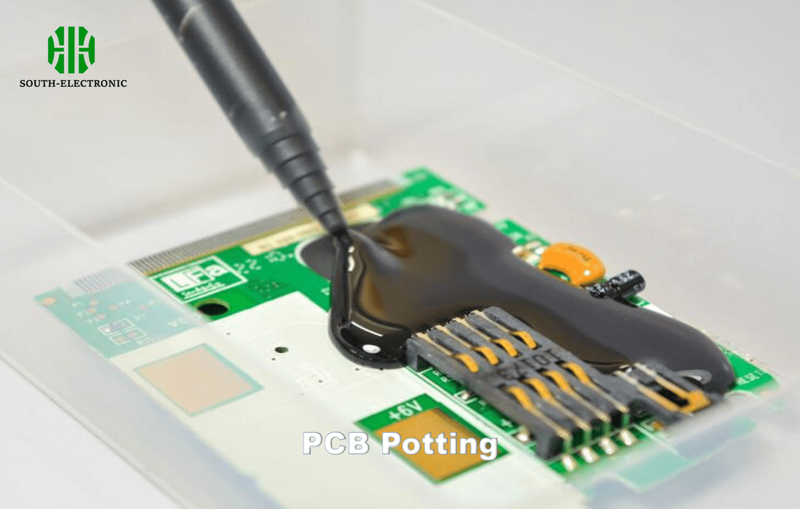
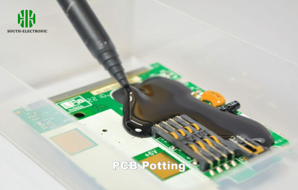
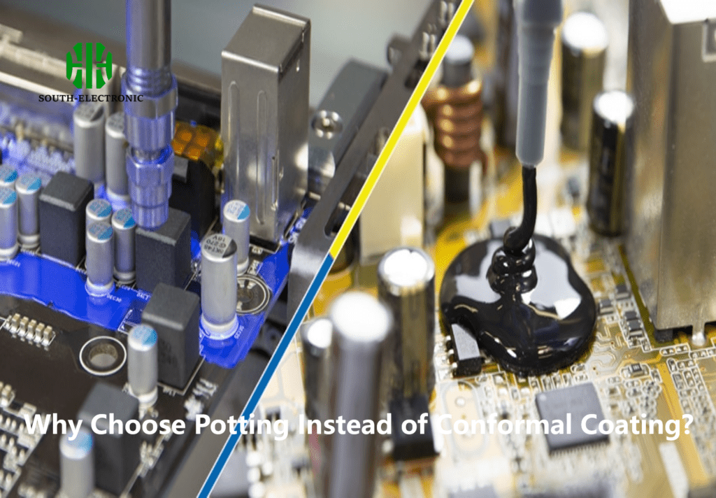
Potting involves pouring liquid resin into a mold containing PCB assemblies, then curing it into a solid shield against moisture, chemicals and shocks. It creates complete encapsulation unlike surface-level coatings.
Now let’s explore key decisions around potting versus other methods, perfecting the process, and avoiding hidden pitfalls in this essential protection technique.
Potting[^1] PCB vs. Conformal Coating[^2]: Which Protection Does Your Electronics Really Need?
Shock damage just cost me $3k on field equipment. You face heartbreaking failures too if environmental hazards breach weak defenses. Why gamble with partial coatings?
Potting submerges entire assemblies in protective resin, while thin conformal coatings just add a surface layer. Use potting against extreme stresses like immersion or constant vibration; choose coatings for stable indoor applications needing component access.
Selecting the Right Shielding Strategy
Electronic protection isn’t one-size-fits-all. Critical criteria include operational environment, repairability needs, and budget constraints. Based on my projects, ask:
Three Non-Negotiable Questions
| Criteria | Potting Solution | Coating Alternative |
|---|---|---|
| Moisture Threat[^3] | Submersion-proof | Resists humidity only |
| Impact Resistance[^4] | Shock absorption matrix | Surface scratch protection |
| Maintenance Needs[^5] | Permanent encapsulation | Re-workable with solvents |
Coatings suit prototypes needing component swaps or indoor devices like thermostats. Potting[^1] battles harsh environments: factory robots, marine sensors, or vehicle trackers must endure water intrusion and crushing vibrations. One construction monitor failed after coating struggled with daily foot traffic vibrations – but potting solved the rattle. Evaluate stress levels brutally.
How to achieve a perfect seal in the PCB potting process?
Air bubbles trapped under my resin caused premature corrosion in humid Brazil. It taught me: flawless potting demands precision in preparation and execution.
Perfect sealing requires degassed resin poured slowly at 20-30° angle in vibration-free environments. Strategic heating during curing ensures bubble-free adhesion. Clean surface prep is essential.
Mastering Bubble-Free Encapsulation
Voids become moisture highways. Achieving hermetic sealing involves three critical stages I learned deploying telematics units:
Precision Steps for Reliability
| Stage | Best Practice | Common Pitfalls |
|---|---|---|
| Preparation | Clean surface with plasma treatment | Fingerprint oil contamination |
| Pouring | Slow, continuous stream from one edge | Rushed pouring trapping air |
| Curing | Ramping temperatures ±5°C/min | Uneven heating causing cracks |
Always pre-heat components to match resin temperature. That solar controller project? Room-temperature boards caused cracked shells during thermal cycling when resin contracted faster than PCBs. Patient, angled pouring reduces trapped bubbles – I use syringes for intricate boards. Microscopic gaps lose wars against condensation.
My warehouse held 200 potted boards ruined by curing miscalculations. Beyond material prices lurk expensive traps: process failures and return logistics drain budgets.
Potting costs include extra labor (20-40%), failed batch scrap (5-15%), and testing apparatus. Resin shrinkage and thermal stress create chronic reliability issues, while rework means destroying assemblies.
Counting the Real Price Tag
Initial calculations often overlook compounding factors:
Cost Breakdown of Unexpected Consequences
| Expense Category | Typical Impact | Mitigation Strategies |
|---|---|---|
| Process Setup | Mold customization fees | Standardize housing designs |
| Long Cycles | Curing time bottlenecks | Invest in faster-set epoxies |
| Material Waste[^6] | Foaming/over-pour 5-8% resin | Vacuum mixing chambers |
| Failure Costs | Field returns + recalibration | Environmental testing chamber |
Material cost considerations extend beyond resin per liter. Failed medical devices taught me: air-cargo returns chew savings from cheap resins instantly. Thermal mismatch strains dominate failure statistics. I now prototype at lifecycle temperature ranges – your production saves months with stress-test data.
How to prevent voids and cracks in potted PCBs?
Wrecked aerospace tests ($$) traced to micro-cracks. Voids become water reservoirs in temperature swings. Both demand disciplined process controls to avoid.
Prevent voids by degassing resin mixes and pouring in vacuum chambers. Stop cracks with resin-CTE matching PCB materials. Adding silica fillers reduces shrinkage.

Engineering Flawless Encapsulation
Cracked seals fail incrementally. Address formation mechanisms through material science and physics:
Battling Imperfections at Scale
| Failure Mode | Primary Cause | Solution Path |
|---|---|---|
| Voids | Trapped air/gases during pour | Vacuum processing pre/post pour |
| Delamination | Poor surface adhesion | Surface-activating primers |
| Thermal Cracks | CTE resin > copper traces | Flexibilizer resins + fillers |
| Cure Stress | Over-accelerated reactions | Controlled multi-stage curing |
Exhaustive defoaming remains critical. That submersible sensor project revealed: under-vacuum times create bubbles while excessive cycles cause premature gels. Use CTE-matched epoxies – my industrial controls gained longevity with silicone-based resins flexing around rigid components. Monitor curing like a baker watching bread.
Conclusion
PCB potting builds vital environmental armor but demands technical awareness of materials, process pitfalls, and cost management in protective strategies (max 40 words).
[^1]: Explore the benefits of potting for electronics protection and understand its importance in harsh environments.
[^2]: Learn how conformal coating differs from potting and when to use each method for optimal protection.
[^3]: Discover the impact of moisture on PCBs and why moisture-proofing is crucial for longevity.
[^4]: Find out how to improve impact resistance in PCBs to prevent damage from shocks and vibrations.
[^5]: Understand the maintenance implications of potting versus conformal coating for your electronic devices.
[^6]: Learn strategies to reduce material waste during potting, enhancing efficiency and cost-effectiveness.