

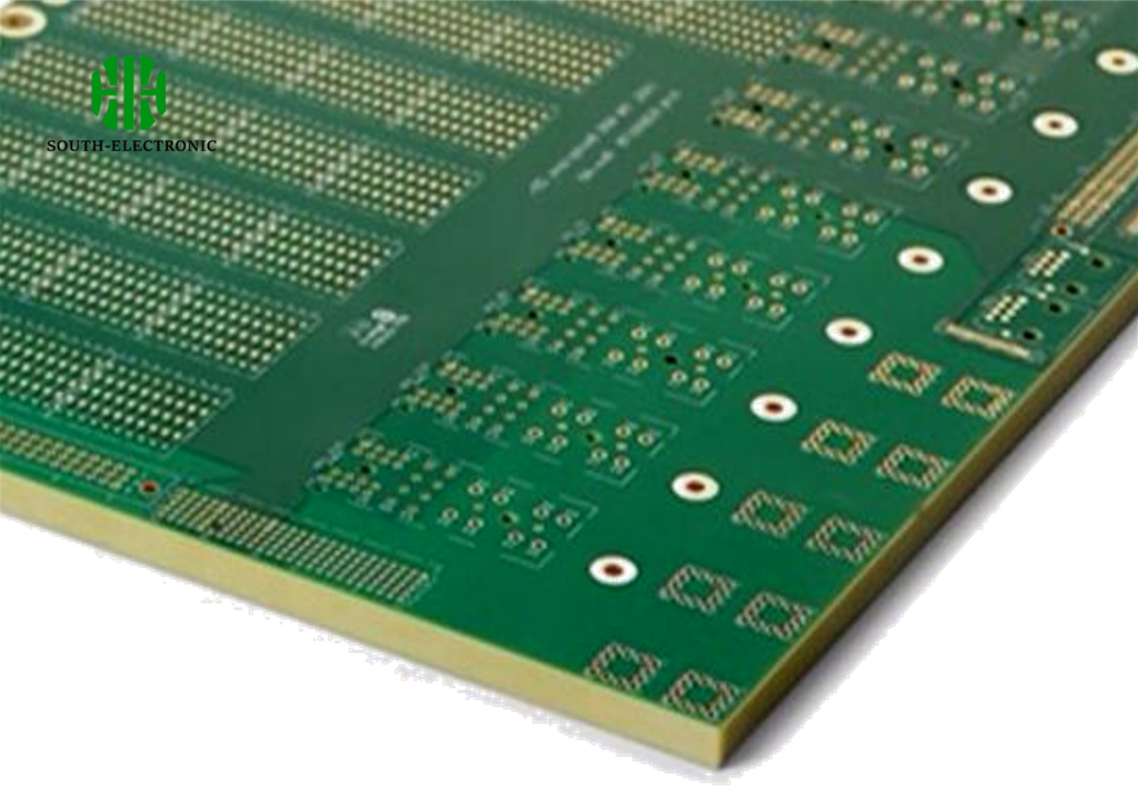
Choosing the wrong PCB thickness can ruin your circuit board. This mistake causes mechanical failures and connection problems. Understanding standard thicknesses prevents design disasters.
The most common standard PCB thickness is 1.57 mm (0.062 inches), derived from early materials like plywood. Other standards include 1.0 mm for lightweight devices and 2.36 mm for industrial equipment. You’ll need thicker boards for heavy components or high-power applications.

Now you know the basics, but thickness impacts more than just measurements. Let’s examine how it connects to real design choices.
How to choose the right PCB thickness for your project?
Mismatched board thickness breaks your device assembly. Mechanical stress accumulates causing cracks. Focus on these core requirements first.
Select thickness around mechanical space and layer count. Prioritize connector compatibility and bend tolerance. High-power circuits need thicker boards for heat dissipation and stability while slim devices save space with thinner PCBs.

Three Key Selection Factors
Think about each design aspect separately:
Device Constraints
Physical measurements matter most. Thin PCBs under 1mm fit wearable tech. Thick 3mm boards support heavy transformers. Measure case dimensions first. Your enclosure space decides minimal thickness. Bending requirements also matter. Flexible circuits need thinner cores.
Layer Stack Complexity
Layer counts change thickness needs:
| Layer Count | Recommended Thickness | Reason |
|---|---|---|
| 1-2 Layers | 1.0-1.6mm | Standard range |
| 4-6 Layers | 1.6-2.0mm | Prevents lamination voids |
| 8+ Layers | Over 2.36mm | Material stability |
Performance Requirements
Power handling changes with thickness:
- Thin boards (under 1mm) handle less than 5A power
- Standard 1.57mm works for 5-10A circuits
- Thick 2.36mm+ boards manage 20A+ without heat issues
Signal quality also depends on thickness. High-frequency signals need precise impedance control. Thicker dielectrics allow better impedance matching for RF designs.
How does board thickness impact cost, power, and signals?
Using thick boards unnecessarily wastes money. Material costs jumps 30% at 2mm thickness versus 1.6mm. Thin boards create heat risks during assembly. Check all three impact areas.
Thicker PCBs cost more but withstand higher power loads. Thin boards cause impedance issues in high-speed circuits. Every 0.5mm increase adds 25% material cost while improving thermal performance by 15%.

The Triple Trade-Off
PCB thickness creates unavoidable compromises:
Cost Factors
Material spending increases linearly with thickness. Processing costs also rise:
- Drilling time doubles for 2mm vs 1mm boards
- Lamination cycles take 20% longer
- Copper usage increases 30% at 2oz weight
| Power Handling Rules Thermal management depends on board bulk: |
Thickness | Heat Capacity | Suitable Applications |
|---|---|---|---|
| 0.8mm | Low | Battery sensors | |
| 1.57mm | Medium | Consumer electronics | |
| 3.0mm | High | Motor controllers |
Signal Behavior Changes
Traces act differently at varying heights:
- Thin boards struggle with impedance below 4GHz frequencies
- Standard thickness maintains signal integrity up to 10GHz
- Thick boards distort high-speed signals through vias
Signal loss increases 0.5db per millimeter thickness in RF circuits. Controlled impedance designs need thickness consistency within ±10%.
How thick is a standard 2 layer PCB?
Designing a 2 layer PCB? Wrong thickness causes connector fails. I recall a prototype that wouldn’t slot into its interface. The standard avoids such disasters.
Most 2 layer PCBs use 1.57mm (0.062") thickness. This matches universal connector depths like PCIe slots. Alternate thicknesses include 1.0mm for portable gadgets and 2.0mm for power converters needing extra rigidity.
Why 1.57mm Dominates
Several factors maintain this standard:
Manufacturing Ecosystem
Over 90% of fabricators stock 1.57mm materials. Production lines calibrate machinery for this thickness. Deviations cause fabrication delays and extra costs.
Mechanical Considerations
Thin 1.0mm boards flex during soldering. Thicker 2.0mm options waste material. The 1.57mm standard balances:
- Component weight support
- Assembly process stability
- Connector compatibility
| When to Deviate Select alternatives for special cases: |
Thickness | Use Case | Benefit |
|---|---|---|---|
| 1.0mm | Wearable trackers | Space savings | |
| 2.0mm | High-vibration machinery | Vibration resistance | |
| 1.57mm | General purpose devices | Cost efficiency |
Edge connectors demand strict thickness control. PCIe slots tolerate just ±0.1mm variation. Confirm interface specs before selecting non-standard options.
Conclusion
PCB thickness affects cost, performance, and reliability. Default to 1.57mm for most projects. Choose alternatives only when special requirements demand them.

