

You lost money on your last PCB run. Wasted material bloated your costs. Standard panel sizes solve this but few engineers use them right.
Common standards like 18×24" or 12×18" balance material efficiency and machine compatibility. There’s no universal size – your fabrication equipment and PCB dimensions decide the best fit. Always maximize board count per panel to cut waste.
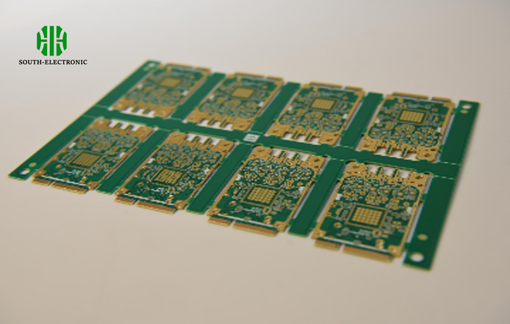
Understanding panel standards is just step one. How you break those panels apart drastically impacts your bottom line. Keep reading to uncover hidden cost traps.
How does breakaway method (V-score/tab routing) affect panel size design?
Fragile circuits snapping during separation? That’s your breakaway method failing. Poor choices here force panel size compromises and raise failure rates.
V-scores need 0.5" edge clearance, shrinking usable space. Tab routing adds tooling time but allows tighter layouts. Always confirm your fabricator’s capabilities before finalizing panel dimensions.
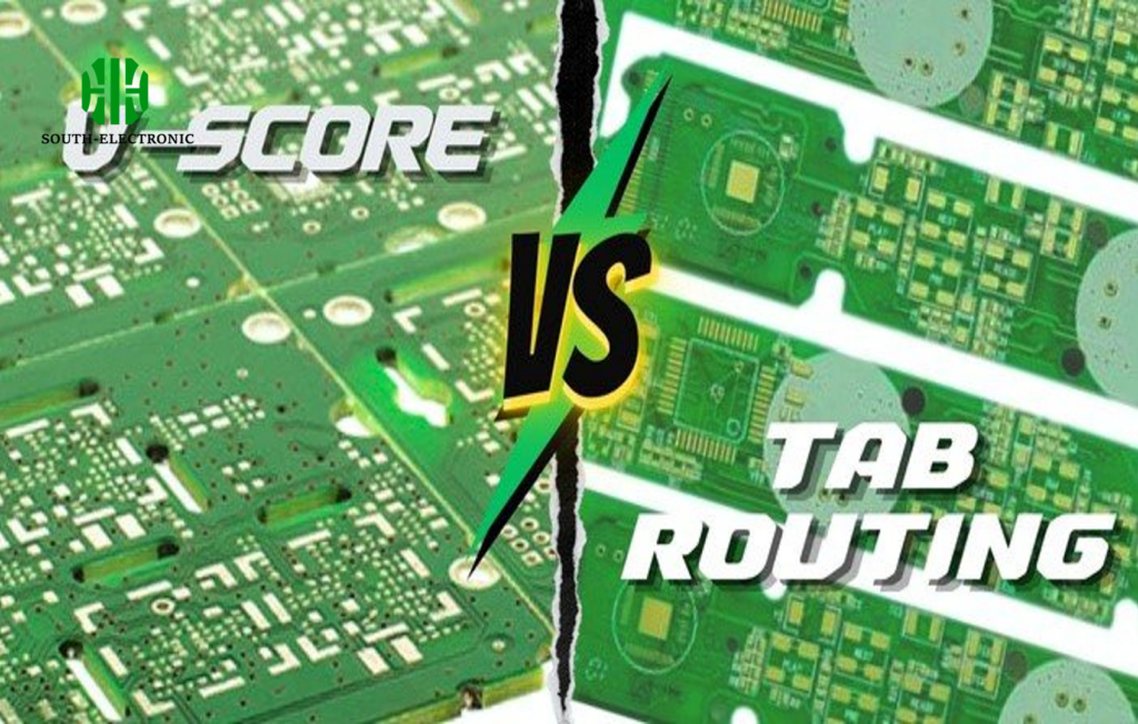
Breakaway Method Design Rules
Your panel isn’t just a carrier – it’s part of the manufacturing process. Choose breakaway methods based on three factors:
| Feature | V-Score Pros | Tab Routing Pros |
|---|---|---|
| Space Needed | Needs wider borders (reduces usable area) | Minimal waste between boards |
| Cost Impact | Faster but limited layout options | Higher tooling cost per panel |
| Best For | Rectangular boards with no edge components | Complex shapes or sensitive components |
Thin PCBs under 0.8mm often crack along V-scores during depaneling. I learned this the hard way on a wearable project – 23% of boards fractured. Tab routing with 2mm spacing solved it but increased panel costs by 15%. Balance reliability and cost by testing small batches first.
Material costs spiked 40% on your last order? That’s waste eating profits. Standard 18×24" panels hide inefficiencies if you don’t optimize layouts.
Small gaps between boards compound waste exponentially. An extra 2mm spacing on a 18×24" panel can waste $127 per 100 panels. Match your board dimensions to panel standards for optimal yield.
Waste Reduction Tactics
Waste costs hide in blank panel edges and routing channels. Consider these in your design phase:
| Waste Source | Cause | Mitigation Strategy |
|---|---|---|
| Border Loss | Machine clamping margins | Design boards < panel size by 0.3" |
| Grid Gaps | Incorrect spacing calculations | Use panelization software for accuracy |
| Bad Fits | Mismatched board dimensions | Adjust board aspects to maximize yield |
I once redesigned a sensor array from 8 to 11 boards per 12×18 panel by rotating components. Material costs dropped 31%. Fabricators charge for full panels – every empty square inch is your lost money. Always demand utilization reports before mass production.
What are the top 5 panelization mistakes to avoid for standard sizes?
5am factory call: "Your panels won't fit our printer." Your panel edge clearance failed. Avoid these common errors that trigger delays and rework fees.
Critical errors include ignoring tooling holes, incorrect spacing, and mixed board orientations. Use fiducials consistently and verify breakaway tabs exceed 0.8mm thickness. Always submit panel files for pre-check.

Mistake Breakdown and Fixes
Don’t learn through costly failures. Steer clear of these pitfalls:
| Mistake | Consequence | Prevention |
|---|---|---|
| No Tooling Holes | Misaligned assembly | Add 3+ 3mm holes within 1° tolerance |
| Mixed Orientations | Failed automated soldering | Keep components facing one direction |
| Undersized Tabs | Boards detaching during assembly | Maintain 1mm min tab width |
| Missing Fiducials | Pick-and-place errors | Place copper markers at 2 corners |
| Overcrowding | Breakaway damage | Leave 20% free space between boards |
I saw a client ignore fiducial placement. Their assembly house charged $2,800 for manual alignment. Simple panel marks would have avoided this. Remember: your fabricator sees hundreds of designs – their feedback is gold. Send panel drawings before finalizing.
Conclusion
Standard PCB panels like 18×24" or 12×18" reduce waste when optimized. Choose breakaway methods wisely, minimize gaps, and avoid layout errors to slash hidden costs.

