
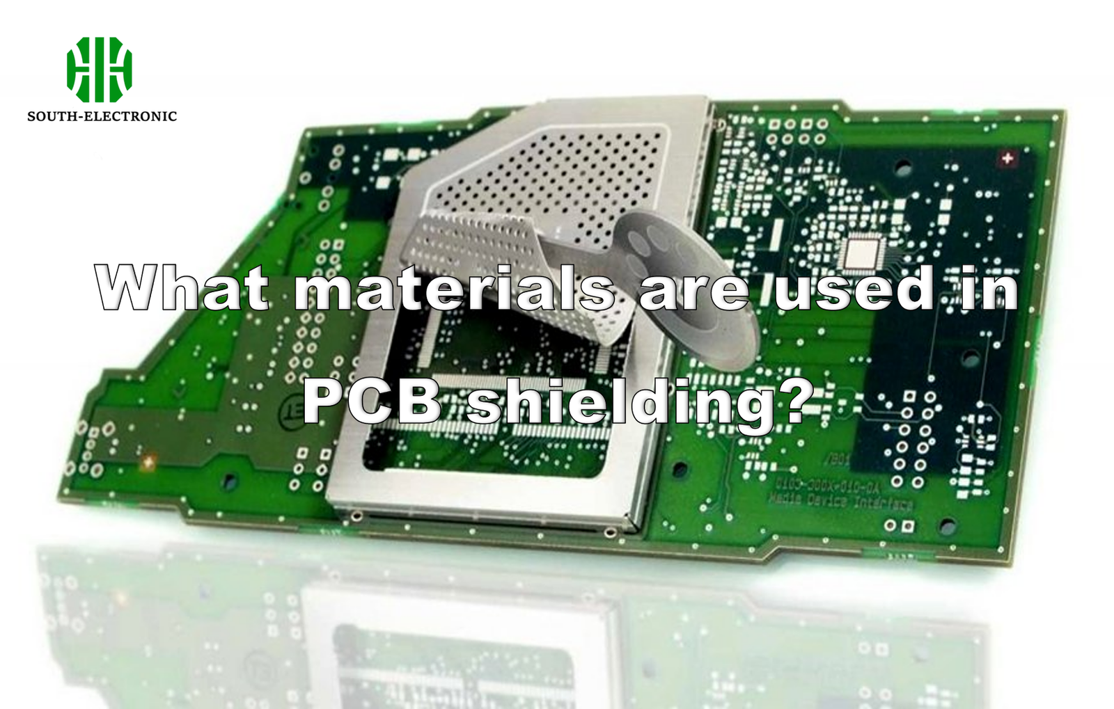
Is electromagnetic interference crippling your electronics? Unshielded circuits face signal loss and data corruption. Choosing the right shielding material solves these invisible threats quickly.
Common PCB shielding materials include copper and nickel silver alloys for peak performance, plus cost-effective tin-plated steel or aluminum. These block electromagnetic interference (EMI) through metal cans, conductive coatings, and specialized tapes or meshes.
Now you know the materials, but material selection is just the first step. Let’s explore shield types, smart design choices, and proven testing methods to ensure complete protection for any project.
What are the common types of PCB shields?
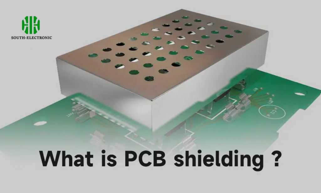
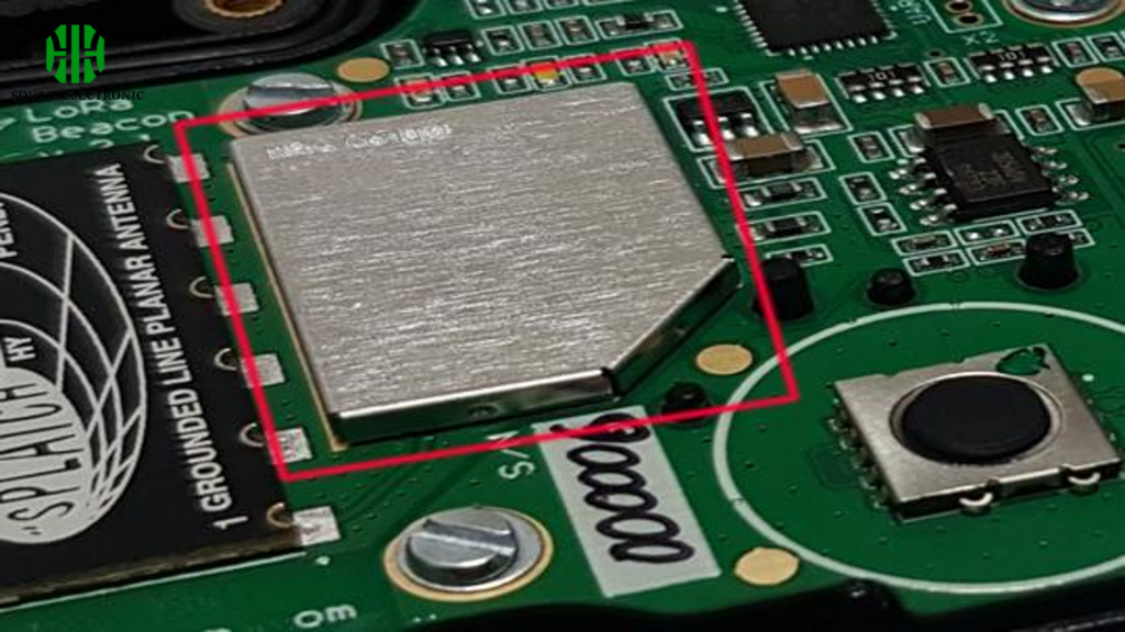
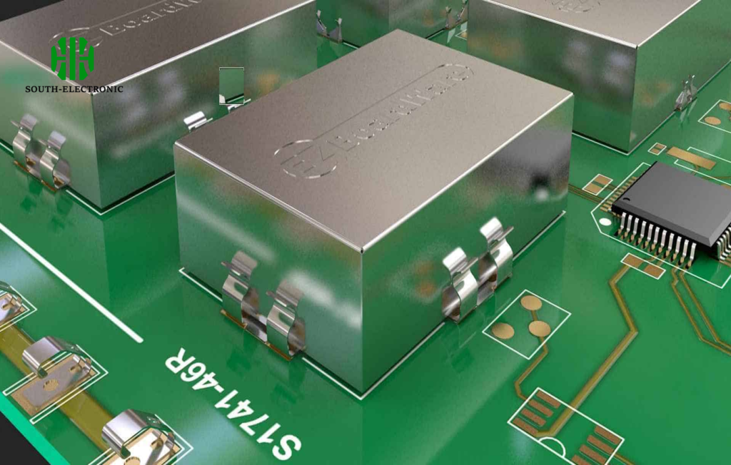
Ever seen strange metal boxes on circuit boards? These PCB shielding cans directly block electromagnetic noise. But cans are just one solution among several techniques.
Four primary shield types exist: solid metal enclosures ("cans"), conductive coatings (spray or paint), adhesive tapes with conductive layers, and flexible wire mesh gaskets. Cans offer maximum isolation while coatings suit space-limited designs.
Comparing Shield Type Performance
Understanding each type’s strengths helps match them to your specific EMI challenges.
| Shield Type | Best For | Limitations | Typical Materials |
|---|---|---|---|
| Metal Enclosures (Cans) | Board-level isolation | Fixed size, limits access | Tin-plated steel, aluminum |
| Conductive Coatings | Complex shapes, flexibility | Lower durability | Copper/nickel acrylic sprays |
| Adhesive Shielding Tapes | Quick repairs, connectors | Weaker at high frequencies | Copper foil with conductive adhesive |
| Wire Mesh Gaskets | Irregular surface gaps | Compression maintenance needed | Nickel-plated copper braid |
PCB shielding techniques vary widely – cans excel for Arduino projects needing robust isolation, while coatings work better behind curved smartphone displays. Tapes bridge small gaps effectively but fail at high GHz frequencies. Meshes handle vibration-prone areas beautifully. Your choice balances cost versus frequency needs.
What are critical design points for PCB shields?
Think your shield will work just because it’s metal? Think again. Even premium materials perform poorly with flawed basic design execution.
Ignored gaps create "EMI leakage spots." Vital rules? Ensure full ground plane contact and maintain shield continuity. Remember: gaps under 1/20th wavelength block targeted frequencies.
Three Pillars of Effective Shield Design
Poor grounding turns shields into antennas. These principles prevent disaster:
-
Grounding Connection
Use multiple solder points around the shield perimeter. Every centimeter without contact reduces effectiveness by 15%. -
Seam Management
Overlapping joints work better than butted edges. For enclosures, add conductive gaskets where panels meet. -
Thermal/Vibration Planning
Metals expand differently than FR4 boards. Allow 0.3mm thermal gaps to avoid stress fractures during soldering.
pcb shielding cans demand particular precision – solder pads must completely surround their base. One break invites EMI. For coatings, thickness uniformity matters. Apply at least 25μm for 1GHz protection. Arduino projects often fail shielding because ventilation holes lack embedded wire meshes.
How to test PCB shield effectiveness?
Finished assembling your shield? Congratulations – now prove it works. You cannot see or hear electromagnetic problems building slowly inside shielded areas.
Two primary testing methods exist: chamber scans measure overall emissions, while near-field probes pinpoint leakage hotspots. Tests compare readings with/without shields to confirm performance.
Validating Real-World Protection
Laboratory-grade validation ensures your PCB shielding techniques deliver:
Radiation Testing (EMI Chambers)
- Measures electromagnetic waves escaping the device
- Tests comply with FCC/CE standards
- Costs $200-$1000 per hour but provides certification data
Probe-Based Detection
- Using handheld magnetic/electric field probes
- Maps specific weak spots (joints/vents/components)
- Affordable kits under $500 for DIY diagnostics
I run basic emission scans for all Arduino shield designs. Surprisingly, many "protected" boards show 30% leakage at can seams. If your budget allows only one test, scan the final product. Probe testing suits debugging. Effective emi shielding shows >15dB attenuation from baseline.
Conclusion
Smart PCB shielding combines material science with precision design and thorough testing. Protect devices by matching metals to challenges and verifying real-world performance.

