

When I first stepped into the world of PCB design, I was both excited and overwhelmed. The field seemed vast, with so much to learn and master. But I knew that having clear goals and a structured path would be key. Technical experts say there are seven core knowledge areas to focus on. Let me share how I approach each of them, based on my own experiences and learning journey.
1. Mastering at Least One Mainstream EDA Tool
There are many PCB design software. Currently, the main ones used in the market include the following four: Cadence Allegro, Mentor EE, Mentor Pads, Altium Designer, Protel, etc. Among them, Cadence Allegro has the highest market share. Allegro has many advantages, such as a user-friendly software interface, fast response speed, high operational efficiency, rich secondary development functions, a complete rule manager, and powerful dedicated high-speed design functions, etc.
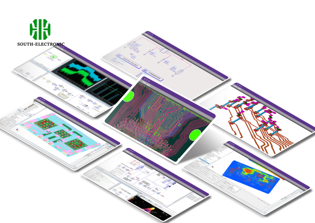
The first step I took was to choose an EDA tool to specialize in. After researching, I decided on Cadence Allegro, which has the highest market share in the industry. I heard from seniors that it’s widely used in communication, server, and industrial control fields, which aligns with my interest in complex projects.
2. Understanding Components, Schematics, and Key Signals
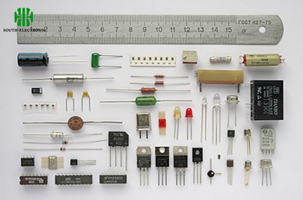
Common electronic components: resistors, capacitors, inductors, transformers, diodes, transistors, field-effect transistors, optocouplers (OC), sensors, crystal oscillators, relays, buzzers, rectifier bridge stacks, filters, switches, fuses, etc. The key signals include: power supply, simulation signal, high-speed signal, clock signal, differential signal, synchronization signal, etc.
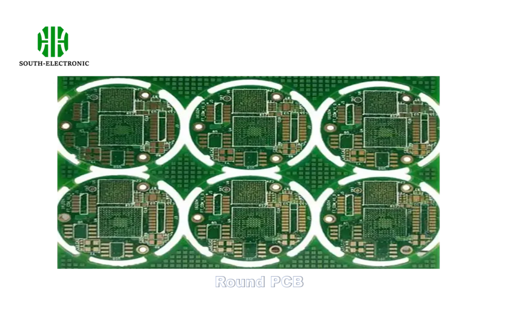
3. Familiar with board materials, processes and techniques
Common boards: cardboard, semi-fiberglass board, FR-4 fiberglass board, aluminum substrate, etc.
Core process technology of circuit board factory: cutting, drilling, plated through hole (PTH), circuit production, solder mask technology
4. Familiar with SMD plug-in assembly processes and techniques
Surface mount technology (SMT) process flow: solder paste printing, component mounting, reflow soldering, AOI inspection
Technical advantages: high-density integration (supporting 0.3mmPitch IC), high reliability, suitable for automated production, widely used in smartphones and laptop motherboards.
Through hole plug-in technology (THT) process flow: component plug-in, wave soldering, shearing cleaning, technical characteristics, mixed assembly process
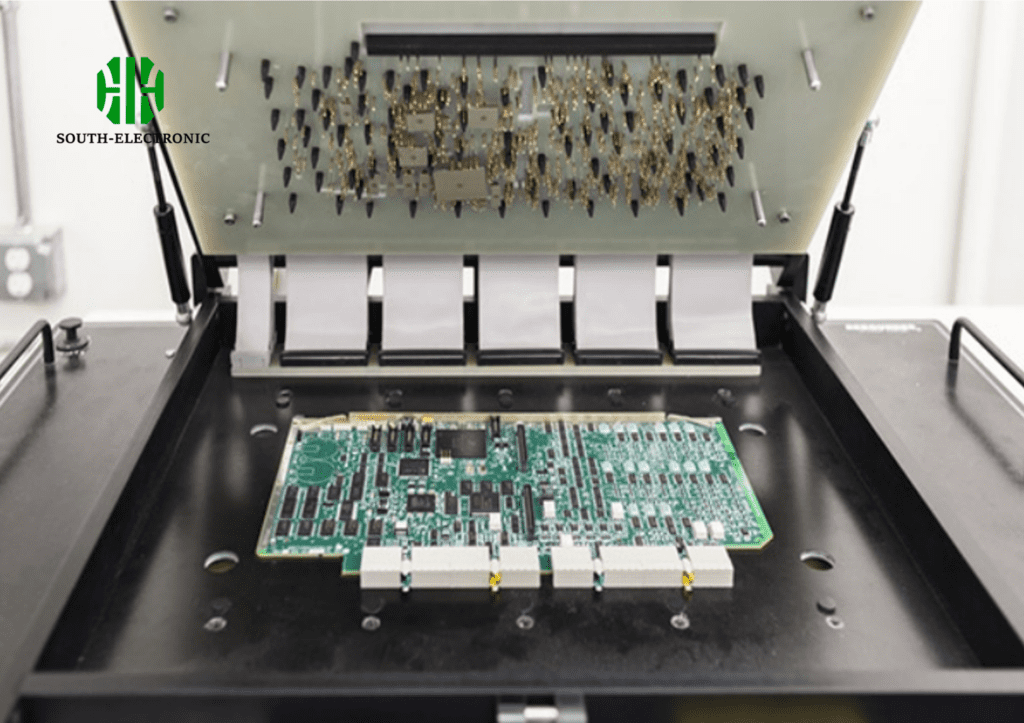
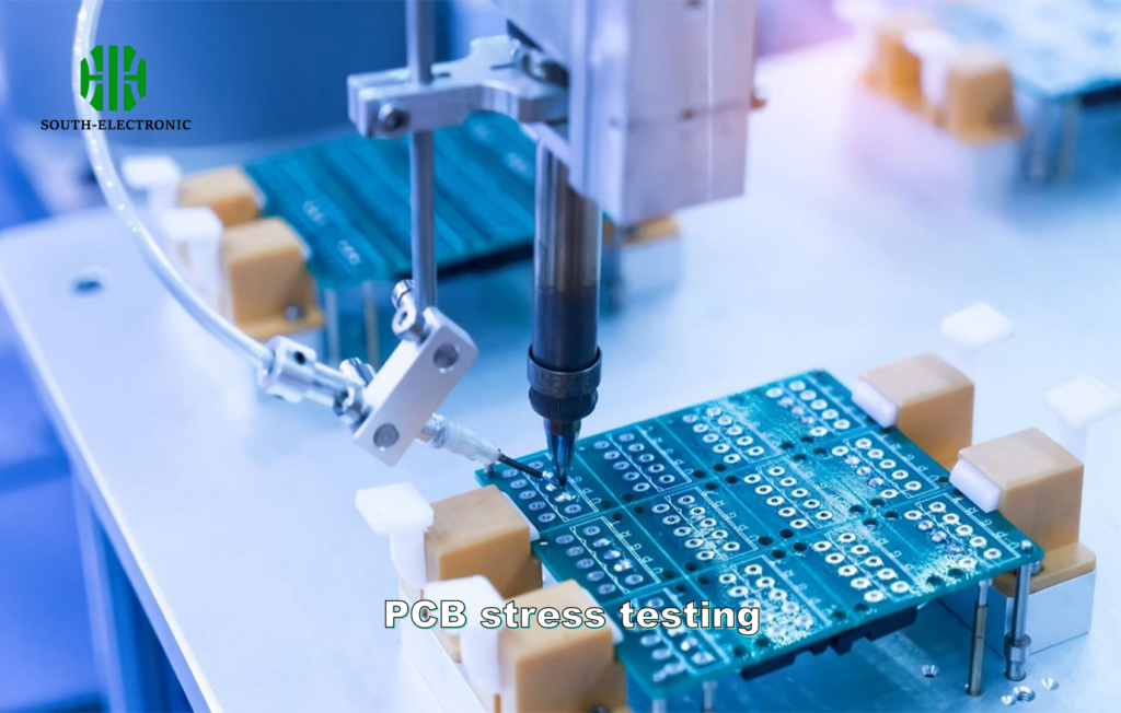
5. Familiar with welding tests
Solderability testing is generally used to make a qualitative and quantitative evaluation of the solderability of components, printed circuit boards, solders and fluxes. In the assembly and welding process of electronic products, the quality of welding directly affects the quality of the whole machine. Therefore, in order to improve the welding quality, in addition to strictly controlling the process parameters, it is also necessary to conduct scientific solderability tests on printed circuit boards and electronic components.
6. Have a certain understanding of SI/PI knowledge
With the increase in the output switching speed of integrated circuits and the increase in the density of PCB boards, signal integrity (SI) has become one of the issues that must be concerned about in high-speed digital PCB design. Factors such as the parameters of components and PCB boards, the layout of components on PCB boards, and the wiring of high-speed signals will cause signal integrity problems, resulting in unstable system operation or even no operation at all. How to fully consider the factors of signal integrity in the design process of PCB boards and take effective control measures has become a hot topic in today’s PCB design industry.
Under the development trend of high power consumption, high density, high speed, high current and low voltage in electronic systems, the power integrity (PI) problem in the field of high-speed PCB design has also become increasingly serious.
As an excellent PCB design engineer, of course, you need to have a certain understanding of SI/PI knowledge to guide the optimization of PCB design, improve power channel design, optimize decoupling capacitor design, etc.
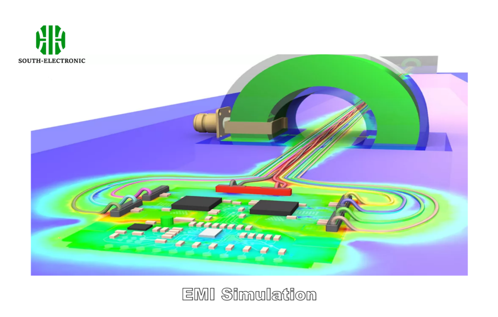
7. Have a deep understanding of EMC/EMI knowledge of the designed product PCB
As we all know, the design of PCB should comprehensively consider multiple factors such as function realization, cost, production process, EMC, and aesthetics.
As the frequency of electronic signals and processors of electronic equipment continues to increase, the electronic system has become a complex device containing multiple components and many subsystems. High density and high speed will increase the radiation of the system, while low voltage and high sensitivity will reduce the anti-interference of the system. Therefore, electromagnetic interference (EMI) is a real threat to the safety, reliability and stability of electronic equipment. When we design electronic products, the design of PCB boards is crucial to solving EMI problems.
Conclusion
Becoming an excellent PCB engineer is a continuous learning process. From mastering EDA tools to understanding complex SI/PI and EMC concepts, each step requires practice, patience, and a willingness to learn from mistakes. If you’re just starting out, remember: focus on building a strong foundation in these seven areas, learn from every project, and don’t be afraid to ask for help. With time and effort, anyone can become a skilled PCB engineer.

